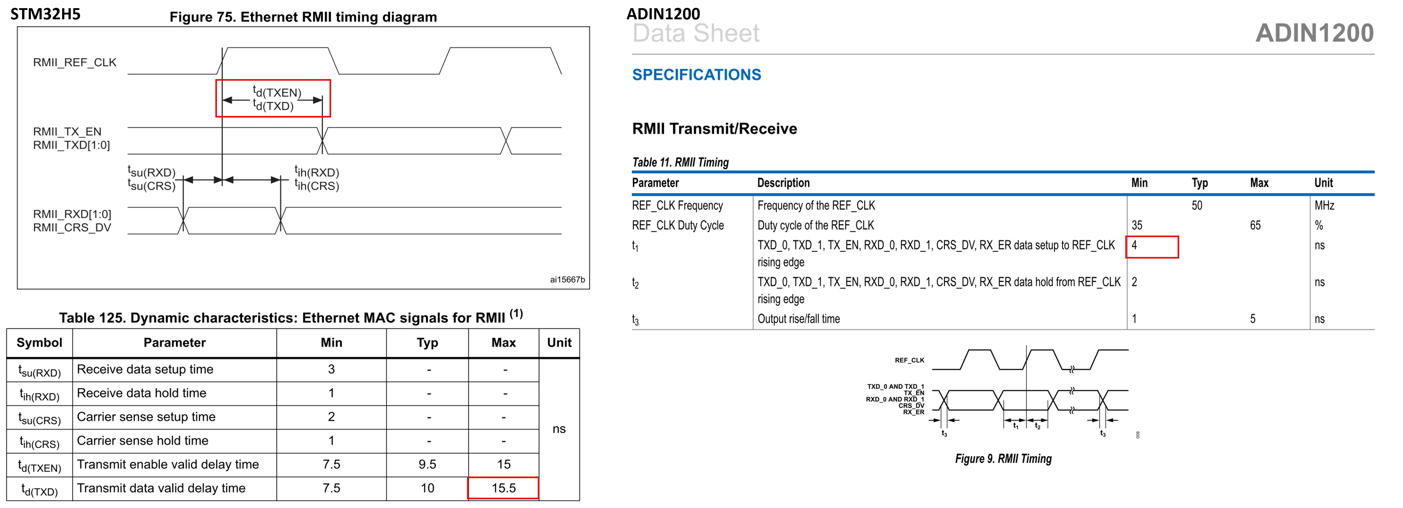
STM32H563–ADIN1200 RMII timing margin
Hello,
We are currently designing a board using an STM32H563VI and an ADIN1200 Ethernet PHY. The design is still at an early stage, and no prototype hardware has been built yet, so we can still change the interface from RMII to MII if necessary.
The planned RMII conditions are as follows:
* RMII reference clock: 50 MHz
* I/O voltage: 3.3 V
* STM32 GPIO speed: OSPEEDR = 10 (High speed)
* I/O compensation cell: Enabled
* ADIN1200 minimum setup time: 4 ns
* ADIN1200 minimum hold time: 2 ns
* Application ambient temperature range: −20°C to +50°C
According to the STM32H563 datasheet, the maximum delay from the RMII_REF_CLK rising edge to TXD[1:0]/TX_EN valid is 15.5 ns. Therefore, the worst-case setup margin appears to be:
20 ns − 15.5 ns − 4 ns = 0.5 ns
This calculation leaves only 0.5 ns of margin before considering PCB trace skew, capacitive loading, and the difference between the STM32 timing measurement threshold of 0.5 × VDD and the RMII/ADIN1200 timing thresholds.
This is my first time designing an RMII interface, so I am not sure whether a calculated worst-case setup margin of only 0.5 ns is acceptable in a practical PCB design.
Can ST confirm whether the RMII timing between the STM32H563 and ADIN1200 can be guaranteed over the operating voltage and temperature range under these conditions? If sufficient timing margin cannot be guaranteed, would ST recommend changing the design to MII?
Thank you for your support.