

MagSense
Associate III
August 12, 2020
Question

SPI – bit shift issue in MISO line of STM32F303x (Slave) - with MOSI unaffected

Scenario –

Currently I am using STM32F303CBxx as my slave and an Infineon microcontroller as a master. The communication takes place via SPI with the clock frequency as high as 1.985 MHz (approx.). The master and slave are inside a closed metal compartment, where one of the control unit consumes higher amount of current, as high as 35 A.

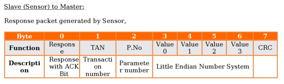
Communication Protocol

The protocol for the communication is as follows.
0693W000003P8RHQA0.png 

Actual Communication and related issue
0693W000003P8RRQA0.png

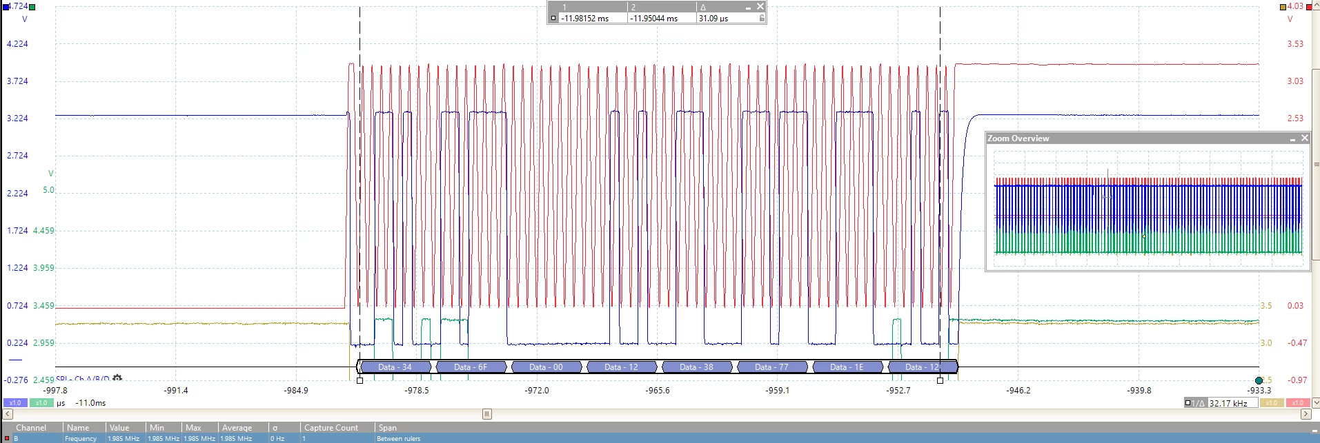
From the above picture (measured data from picoscope), the decoded SPI message from the MISO line is as follows,

0x34 0x6F 0x00 0x12 0x38 0x77 0x1E 0x12

For CRC, I am using the XOR checksum (CRC8). When I check the above message for the validity (using a normal xor checksum calculator online), the xor byte becomes invalid (0x12)

Moreover, the expected message is as follows-> 0x34 0x6F 0x00 0x12 0x38 0x77 0x0F, with a CRC byte value of 0x09.

If I observe the 7th byte -> 0x1E -> 0001 1110, 1-bit shift happened towards the left, as the expected value was 0F -> 0000 1111. This bit shift happens at the 8th byte (CRC) as well.

12 (invalid CRC) -> 0001 0010 (measured) -> 0000 1001 (expected) -> 09 (valid CRC).

The bit-shifting issue happens only on the MISO line of the SPI, when the current consumption is on a higher range (more than 20 A, for example). The clock line does not get disturbed, as I always get valid messages on the MOSI. It should also be noted that the other functionalities of the slave (there are other measurements running in parallel) are unaffected.

This bit-shifting originates most of the time in the 7th or 8th byte of a packet, but rarely occurs in the 1st byte as well.
0693W000003P8WgQAK.png

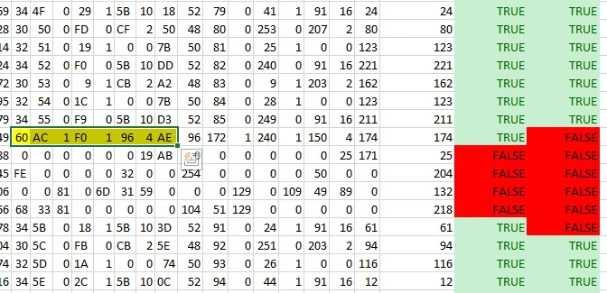
For example, take a look into the above highlighted transaction.

The decoded MISO message is 0x60 0xAC 0x01 0xF0 0x01 0x96 0x04 0xAE. The complete packet is shifted to the left by exactly 1-bit. If I shift the message by 1-bit to the right, I receive the following message -> 0x30 0x56 0x00 0xF8 0x00 0xCB 0x02 0x57. This is a valid transaction and the message holds true.

What could be the source of such bit-shift error? Does this occur in the microcontroller itself?

Any recommendations regarding finding the source of such errors, are highly appreciated.

Please let me know if additional information is required.

Thank you.

This topic has been closed for replies.

38 replies

waclawek.jan
Super User
August 12, 2020

What is the CPOL/CPHA setting?

JW

MagSense
MagSenseAuthor
Associate III
August 12, 2020

Hi,

The CPOL is High (1) and the CPHA is trailing edge (2 edge : 1).

Regards,

MS.

waclawek.jan
Super User
August 12, 2020

On second thought, observing MOSI vs MISO, CPOL/CPHA is probably correct.

The bit shift is most likely caused by the 'STM32 "seing" an extra clock; that this happens "when current consumption is on a higher range" indicates suspected noise/common ground issues.

The depicted SCK slew rate is suspiciously slow.

Try to get a galvanic isolated oscilloscope, placing the oscilloscope's ground clip as close to the STM32's ground as possible, and observe SCK (even stationary), directly on the STM32's pin, during the "high current" or transitions of it. Then try to observe the "glitch" as above. The probe+oscilloscope MUST be fast enough for the slave SPI capabilities, i.e. analog bandwidth above 100MHz and adequate sample rate.

JW

MagSense
MagSenseAuthor
Associate III
August 12, 2020

Hi JW,

I did almost the exact measurement you suggested. I used special shielded cables, which were directly soldered onto the SPI connectors, with GND shield connected to the microcontroller GND. The bandwidth of the oscilloscope I used is around 70 MHz (12-bit resolution).

0693W000003P8tpQAC.png

BLUE -> MISO

RED -> CLK

GREEN -> MOSI

Even I suspected such a "glitch" on the CLK line might be the culprit, but I was unable to capture this on the scope. There, the CLK signals looked fine. Even if we consider that such a glitch occurs on the CLK line, it should affect not only MISO but also MOSI. Right?

waclawek.jan
Super User
August 12, 2020

SCK is generated by master, so it's output (MOSI) is probably derived from internal version of SCK and unaffected (in STM32 it's not this way and MOSI is generated from a feedback from the SCK pin, but that's IMO a deviation, I've never met this approach before).

The SCK is suspiciously slow. slower than MOSI. Is there any way to make it's slew rate higher, maybe a pin setting in a master? Is there any extra hardware on SCK?

JW

MagSense
MagSenseAuthor
Associate III
August 12, 2020

Hi JW,

Thank you for your response. I am using a RC filter at the slave, with a cut-off frequency of 340 MHz and RC Time constant of 5e-10 seconds.

Unfortunately, I cannot change any settings with the master. There are only the RC components on the SCK and nothing else.

Regards,

MS

waclawek.jan
Super User
August 12, 2020

> I am using a RC filter at the slave,

Try to remove it.

JW

prain
Visitor II
August 12, 2020

what is the idle state for clock? in picture it starts from low state but ends with high state. is this correct? make sure no clock edges are ignored.​

waclawek.jan
Super User
August 12, 2020

prain,

> it starts from low state but ends with high state.

Yes I've noticed that too, but CPOL=1, and there is a (barely noticeable) yellow trace which is probably NSS - within it, the clock is already high at the start, so that should be OK.

Also, the bit shift occurs midway in the message. Would the idle state of SCK the culprit, the shift would occur at the beginning.

JW

TDK
August 12, 2020

For a signal at 2 MHz, the edges in your plot look awful. I wouldn't expect an RC filter with a cutoff at 340 MHz to have any affect on them.

"If you feel a post has answered your question, please click ""Accept as Solution""."
Dvorak.Peter
Associate II
August 12, 2020

0693W000003PBNcQAO.png

In the above snip the falling data edge starts out later but arrives before the clock edge

One thing that may work is an RC filter on the data input to match the slew induced delay in the clock signal.

MagSense
MagSenseAuthor
Associate III
August 12, 2020

The error occurs only during a certain "high power consumption" mode (approx. 8 error messages out of 300) and the rest of the time, this error doesn't happen. Wouldn't the RC filter affect the normal operations as well?

waclawek.jan
Super User
August 12, 2020

> I wouldn't expect an RC filter with a cutoff at 340 MHz to have any affect on them.

+1

I'd expect some mistake, like C being 10nF instead of 10pF, or something similar.. Removing the filter (bridging, removing C) should reveal the trough.

Nonetheless, this is a problem only in conjunction with some noise, as the input Schmidt trigger has relatively high hysteresis in 'F3 - typ.100mV for FT and 200mV for TC/TT.

JW

MagSense
MagSenseAuthor
Associate III
August 13, 2020

The capacitors are actually 10pF and I have double checked them.

waclawek.jan
Super User
August 13, 2020

How? Did you physically removed them and measured them?

JW

prain
Visitor II
August 13, 2020

I think a differential signaling method is better in your situation. something like RS422. you can easily make miso, mosi sck , nss lines differential. Transceiver chips like ADM2582 are a good feet for such frequency range

MagSense
MagSenseAuthor
Associate III
August 17, 2020

Thats actually a good solution but unfortunately I cannot leap over from SPI. I have to stick to it. :expressionless_face:Its not in my hands.

Dvorak.Peter
Associate II
August 14, 2020

RE:

The master and slave are inside a closed metal compartment, where one of the control unit consumes higher amount of current, as high as 35 A

 The error occurs only during a certain "high power consumption" mode (approx. 8 error messages out of 300) and the rest of the time, this error doesn't happen.

Can we have more information on the following:

Does the 35A load generate electrical noise ?

Is the sensor connected to STM32F303CB picking up electrical noise ?

Are there any photos of the product available ?

Does the interference stop when the load is disconnected ?

Does the interference stop when the sensor is disconnected ?

Are there any ground loops ?

What is the power source ?

Is the Infineon microcontroller device well documented ?

Are there any noise suppression filters ?

Can you share schematics or block diagram ?

MagSense
MagSenseAuthor
Associate III
August 17, 2020

Does the 35A load generate electrical noise ? -> No actual electrical noise was observed.

Is the sensor connected to STM32F303CB picking up electrical noise ? -> That is the question here. In my answer to @Community member​ , as soon as I reduced the frequency of the GPIO pins, the errors that I observe on MISO line reduced. This might actually tell us something regarding some disturbance on the SPI lines. But the other functionalities of the sensor were unaffected when the error happens.

Are there any photos of the product available ? -> Unfortunately I am not in a position to share this in the forum.

Does the interference stop when the load is disconnected ? -> As mentioned in my initial post, the issue/interference happens only when the control unit is consuming high amount of power. As soon as we step down to a lower stage, the errors do not happen any more.

Does the interference stop when the sensor is disconnected ? -> If the sensor (slave) is disconnected, the communication will also be disconnected. Added to that, the sensor is actually powered by the control unit, which is also powering the master. Hence, If I disconnect the sensor, I will disconnect the power to the sensor as well.

Are there any ground loops ? -> Nothing I know of. The master and the slave share the same ground with no evident ground loops in sight.

What is the power source ? -> Power source is from a standard power supply with 48V input to the control unit. It steps down the voltage to 5V, which is used to power the sensor (slave). The slave has an 3.3V LDO, which is used to power the microcontroller. A similar setup is used on the master side as well. Since the master and the slave are spaced out by a distance of around 15 cm, individual LDOs are used.

Is the Infineon microcontroller device well documented ? -> Yes but unfortunately I do not possess the complete information regarding it. The MOSI and MISO lines are internally pulled up by 1kOhms (by the master controller).

Are there any noise suppression filters ? -> nothing on the SPI lines, apart from the RC filters that were mentioned previously.

Can you share schematics or block diagram ? -> if you need more information, you can specify it. I will try my best to provide them.

0693W000003PQkRQAW.png

Dvorak.Peter
Associate II
August 17, 2020

Thanks for your reply.

Can you shed more light on the mystery 35A load and how is the power adjusted and switched ?

Clearly the the load or its controller is creating some sort of pulse interference.

RE: control unit is consuming high amount of power

Is your control unit a high power (1600W) computing device or a motor drive ?

 Also in the above block diagram the slave should take 5V power and ground from the master

waclawek.jan
Super User
August 17, 2020

> I changed the GPIO pin maximum speed settings (from high to medium) which in-turn reduced the error count to 1 (over 4 seconds measurement).

This is quite surprising and IMO is another indication that ground arrangement is wrong.

JW

MagSense
MagSenseAuthor
Associate III
August 23, 2020

I measured the ground potential between master and the slave, and they seem to be on the same level. So I am not sure If the ground arrangement problem arises here.

waclawek.jan
Super User
August 23, 2020

> I measured the ground potential

DC measurement is worthless in this regard. You are interested in *fast* transients at the moment when the problem occurs (i.e. when the high current is switched or generated or whatever).

JW