

Senior
May 8, 2025
Question

GPIO Latency STM32F411 Blackpill

Hello All, 

I am doing this post after trying everything I can to solve my Issue. 

I have a STM32F411 Blackpill connected on an Apple II Bus Slot.

The Apple II has a clock (Phi0) close to 1 Mhz. Phi0 is connected to Pin A2 where I have setup a Falling & Rising Edge interrupt. 

The GPIO B12 is used to check the latency between each Phi0 phase,

- at the falling edge of Phi0 B13 is clear

- at the rising edge of Phi0 B13 is set, 

I have nothing else running on this STM32, I am observing a delay (avg 335 ns) between the interrupt detection and GPIO set or clear.

Using the logic analyzer: 
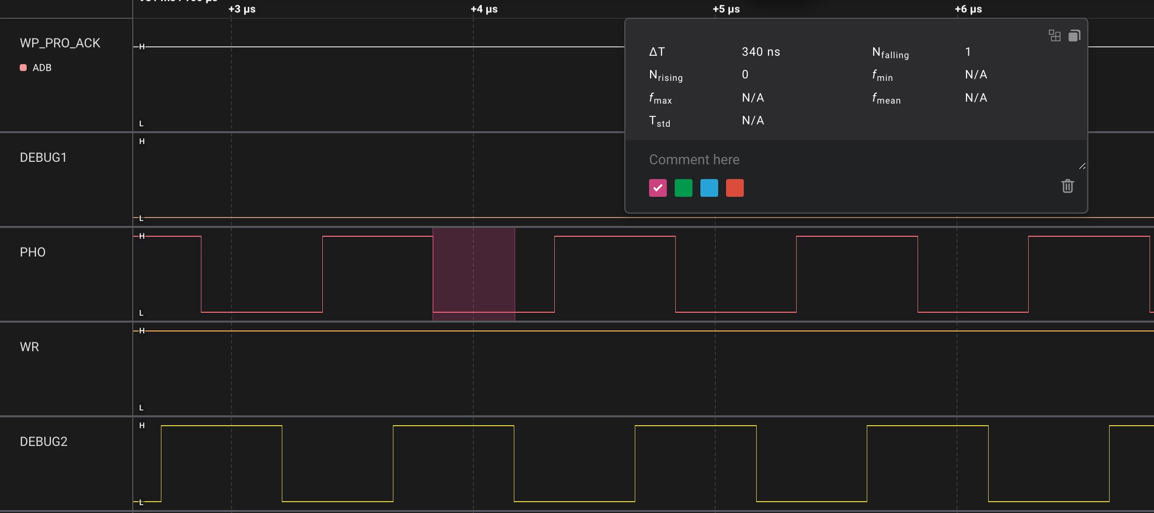
Screen Shot 2025-05-08 at 20.56.06.png

Debug2 is the GPIO B13

I use the following code :

#define GPIO_SET_PIN(port, pin) ((port)->BSRR = (pin))
#define GPIO_CLEAR_PIN(port, pin) ((port)->BSRR = (pin << 16u))

#pragma GCC push_options
#pragma GCC optimize ("-Ofast")

void EXTI2_IRQHandler(void){
 __HAL_GPIO_EXTI_CLEAR_IT(PHI0_Pin);
 if ((PHI0_GPIO_Port->IDR & PHI0_Pin)==0){
 GPIO_CLEAR_PIN(DEBUG1_GPIO_Port,DEBUG1_Pin); 
 }else{
 GPIO_SET_PIN(DEBUG1_GPIO_Port,DEBUG1_Pin); 
 }
}
#pragma GCC pop_options

 The clock setting :

void SystemClock_Config(void)
{
 RCC_OscInitTypeDef RCC_OscInitStruct = {0};
 RCC_ClkInitTypeDef RCC_ClkInitStruct = {0};

 /** Configure the main internal regulator output voltage
 */
 __HAL_RCC_PWR_CLK_ENABLE();
 __HAL_PWR_VOLTAGESCALING_CONFIG(PWR_REGULATOR_VOLTAGE_SCALE1);

 /** Initializes the RCC Oscillators according to the specified parameters
 * in the RCC_OscInitTypeDef structure.
 */
 RCC_OscInitStruct.OscillatorType = RCC_OSCILLATORTYPE_HSE;
 RCC_OscInitStruct.HSEState = RCC_HSE_ON;
 RCC_OscInitStruct.PLL.PLLState = RCC_PLL_ON;
 RCC_OscInitStruct.PLL.PLLSource = RCC_PLLSOURCE_HSE;
 RCC_OscInitStruct.PLL.PLLM = 25;
 RCC_OscInitStruct.PLL.PLLN = 384;
 RCC_OscInitStruct.PLL.PLLP = RCC_PLLP_DIV4;
 RCC_OscInitStruct.PLL.PLLQ = 8;
 if (HAL_RCC_OscConfig(&RCC_OscInitStruct) != HAL_OK)
 {
 Error_Handler();
 }

 /** Initializes the CPU, AHB and APB buses clocks
 */
 RCC_ClkInitStruct.ClockType = RCC_CLOCKTYPE_HCLK|RCC_CLOCKTYPE_SYSCLK
 |RCC_CLOCKTYPE_PCLK1|RCC_CLOCKTYPE_PCLK2;
 RCC_ClkInitStruct.SYSCLKSource = RCC_SYSCLKSOURCE_PLLCLK;
 RCC_ClkInitStruct.AHBCLKDivider = RCC_SYSCLK_DIV1;
 RCC_ClkInitStruct.APB1CLKDivider = RCC_HCLK_DIV2;
 RCC_ClkInitStruct.APB2CLKDivider = RCC_HCLK_DIV1;

 if (HAL_RCC_ClockConfig(&RCC_ClkInitStruct, FLASH_LATENCY_3) != HAL_OK)
 {
 Error_Handler();
 }
}

 The GPIO Settings:

static void MX_GPIO_Init(void)
{
 GPIO_InitTypeDef GPIO_InitStruct = {0};
/* USER CODE BEGIN MX_GPIO_Init_1 */
/* USER CODE END MX_GPIO_Init_1 */

 /* GPIO Ports Clock Enable */
 __HAL_RCC_GPIOC_CLK_ENABLE();
 __HAL_RCC_GPIOH_CLK_ENABLE();
 __HAL_RCC_GPIOA_CLK_ENABLE();
 __HAL_RCC_GPIOB_CLK_ENABLE();

 /*Configure GPIO pin Output Level */
 HAL_GPIO_WritePin(GPIOC, GPIO_PIN_13, GPIO_PIN_RESET);

 /*Configure GPIO pin Output Level */
 HAL_GPIO_WritePin(GPIOA, D_CE_Pin|D_DIR_Pin|IRQ_DRV_Pin, GPIO_PIN_RESET);

 /*Configure GPIO pin Output Level */
 HAL_GPIO_WritePin(GPIOB, DEBUG1_Pin|DEBUG2_Pin|A_CE1_Pin|A_CE2_Pin, GPIO_PIN_RESET);

 /*Configure GPIO pin : PC13 */
 GPIO_InitStruct.Pin = GPIO_PIN_13;
 GPIO_InitStruct.Mode = GPIO_MODE_OUTPUT_PP;
 GPIO_InitStruct.Pull = GPIO_NOPULL;
 GPIO_InitStruct.Speed = GPIO_SPEED_FREQ_LOW;
 HAL_GPIO_Init(GPIOC, &GPIO_InitStruct);

 /*Configure GPIO pins : RW_Pin DEVSEL_Pin */
 GPIO_InitStruct.Pin = RW_Pin|DEVSEL_Pin;
 GPIO_InitStruct.Mode = GPIO_MODE_INPUT;
 GPIO_InitStruct.Pull = GPIO_NOPULL;
 HAL_GPIO_Init(GPIOA, &GPIO_InitStruct);

 /*Configure GPIO pin : PHI0_Pin */
 GPIO_InitStruct.Pin = PHI0_Pin;
 GPIO_InitStruct.Mode = GPIO_MODE_IT_RISING_FALLING;
 GPIO_InitStruct.Pull = GPIO_PULLUP;
 HAL_GPIO_Init(PHI0_GPIO_Port, &GPIO_InitStruct);

 /*Configure GPIO pins : D_CE_Pin D_DIR_Pin IRQ_DRV_Pin */
 GPIO_InitStruct.Pin = D_CE_Pin|D_DIR_Pin|IRQ_DRV_Pin;
 GPIO_InitStruct.Mode = GPIO_MODE_OUTPUT_PP;
 GPIO_InitStruct.Pull = GPIO_NOPULL;
 GPIO_InitStruct.Speed = GPIO_SPEED_FREQ_LOW;
 HAL_GPIO_Init(GPIOA, &GPIO_InitStruct);

 /*Configure GPIO pins : SD_EJECT_Pin RESET_Pin */
 GPIO_InitStruct.Pin = SD_EJECT_Pin|RESET_Pin;
 GPIO_InitStruct.Mode = GPIO_MODE_IT_RISING;
 GPIO_InitStruct.Pull = GPIO_NOPULL;
 HAL_GPIO_Init(GPIOA, &GPIO_InitStruct);

 /*Configure GPIO pins : DA0_Pin DA1_Pin DA2_Pin DA3_Pin
 DA4_Pin DA5_Pin DA6_Pin DA7_Pin */
 GPIO_InitStruct.Pin = DA0_Pin|DA1_Pin|DA2_Pin|DA3_Pin
 |DA4_Pin|DA5_Pin|DA6_Pin|DA7_Pin;
 GPIO_InitStruct.Mode = GPIO_MODE_INPUT;
 GPIO_InitStruct.Pull = GPIO_NOPULL;
 HAL_GPIO_Init(GPIOB, &GPIO_InitStruct);

 /*Configure GPIO pins : DEBUG1_Pin DEBUG2_Pin */
 GPIO_InitStruct.Pin = DEBUG1_Pin|DEBUG2_Pin;
 GPIO_InitStruct.Mode = GPIO_MODE_OUTPUT_PP;
 GPIO_InitStruct.Pull = GPIO_NOPULL;
 GPIO_InitStruct.Speed = GPIO_SPEED_FREQ_VERY_HIGH;
 HAL_GPIO_Init(GPIOB, &GPIO_InitStruct);

 /*Configure GPIO pins : A_CE1_Pin A_CE2_Pin */
 GPIO_InitStruct.Pin = A_CE1_Pin|A_CE2_Pin;
 GPIO_InitStruct.Mode = GPIO_MODE_OUTPUT_PP;
 GPIO_InitStruct.Pull = GPIO_NOPULL;
 GPIO_InitStruct.Speed = GPIO_SPEED_FREQ_LOW;
 HAL_GPIO_Init(GPIOB, &GPIO_InitStruct);

 /* EXTI interrupt init*/
 HAL_NVIC_SetPriority(EXTI2_IRQn, 0, 0);
 HAL_NVIC_EnableIRQ(EXTI2_IRQn);

/* USER CODE BEGIN MX_GPIO_Init_2 */
/* USER CODE END MX_GPIO_Init_2 */
}

Why do I have a huge latency between B13 & PHI0 ?

What can I change / do to reduce that gap ? 

Thank 

Vincent


This topic has been closed for replies.

16 replies

TDK
May 8, 2025

335ns at 100 MHz is 33 ticks. That's about as good as you're going to get with this approach. Might be able to get it down to low 20s.

1) There's a 12-cycle delay for the ISR to fire on the M4 core.

1a) I suspect there are a few clocks of delay between the actual edge and the interrupt becoming pending.

2) There are additional flash wait states if the ISR instruction is not in memory.

3) You have a few instructions before actually setting the GPIO value. These use the same bus to communicate as setting the GPIO. Look at disassembly to see what it's doing.

4) The write to GPIO is not instant and will take a few cycles as well.


You can eliminate (2) by putting instructions in RAM. And you can affect (3), but only slightly.

"If you feel a post has answered your question, please click ""Accept as Solution""."
vbessonAuthor
Senior
May 8, 2025

Hello TDK, 

Thanks, Do you have an example for 2) 

I will try to see the impact 

Vincent


vbessonAuthor
Senior
May 9, 2025

It seems a bit complicated to do it, 

from the reading I did, I need to create a new section in RAM dedicated to ISR VECTOR

then I need to copy the ISR vector to the new section ? 

How do I copy the content if the ISR function to be executed from RAM ? 

Is there an example for F411 ?

Sorry if it seems to be easy... for me it is not

V

vbessonAuthor
Senior
May 9, 2025

I found this article that might help other down the path to put ISR exec in memory, 

https://community.st.com/t5/stm32-mcus/how-to-place-and-execute-stm32-code-in-sram-memory-with/ta-p/49528


I will give it a try to see if it helps toward reducing the latency of ISR execution. 

V


vbessonAuthor
Senior
May 10, 2025

Well, 

I can see using the PC that it is executing from RAM, However it is not reducing the GAP I still have between 340 & 400 ns delay. This is not normal, 

What is wrong with this STM32 ? 

Vincent

TDK
May 10, 2025

Why do you think it is not normal?

What results are you expecting instead?

Did you look at the disassembly? Cortex M4 has (minimum) cycle counts for each instruction. Add them up and compare that to what you're seeing.

"If you feel a post has answered your question, please click ""Accept as Solution""."
vbessonAuthor
Senior
May 10, 2025

I will check the dissassembly, 

It is more like 500 ns  means 50 cycle (OK 12 for the ISR), but stil 38 cycle to trigger a GPIO

seems strange !


vbessonAuthor
Senior
May 10, 2025

this is the content of the dissassembly

465 	EXTI2_IRQHandler:
 466 	.LFB140:
 157:Core/Src/main.c **** 
 467 		.loc 1 157 65 is_stmt 1 view -0
 468 		.cfi_startproc
 469 		@ args = 0, pretend = 0, frame = 0
 470 		@ frame_needed = 0, uses_anonymous_args = 0
 471 		@ link register save eliminated.
 159:Core/Src/main.c **** __HAL_GPIO_EXTI_CLEAR_IT(PHI0_Pin);
 472 		.loc 1 159 3 view .LVU135
 159:Core/Src/main.c **** __HAL_GPIO_EXTI_CLEAR_IT(PHI0_Pin);
 473 		.loc 1 159 6 is_stmt 0 view .LVU136
 474 0000 0E4B 		ldr	r3, .L18
 475 0002 5B69 		ldr	r3, [r3, #20]
 159:Core/Src/main.c **** __HAL_GPIO_EXTI_CLEAR_IT(PHI0_Pin);
 476 		.loc 1 159 5 view .LVU137
ARM GAS /var/folders/22/3r1y38fj3jv6y45lkqfh11sw0000gn/T//ccS6FRfN.s 			page 22


 477 0004 13F0040F 		tst	r3, #4
 478 0008 16D0 		beq	.L15
 160:Core/Src/main.c **** /*
 479 		.loc 1 160 5 is_stmt 1 view .LVU138
 480 000a 0C4B 		ldr	r3, .L18
 481 000c 0422 		movs	r2, #4
 482 000e 5A61 		str	r2, [r3, #20]
 165:Core/Src/main.c **** if (phi0==0){
 483 		.loc 1 165 5 view .LVU139
 165:Core/Src/main.c **** if (phi0==0){
 484 		.loc 1 165 24 is_stmt 0 view .LVU140
 485 0010 03F54443 		add	r3, r3, #50176
 486 0014 1B69 		ldr	r3, [r3, #16]
 165:Core/Src/main.c **** if (phi0==0){
 487 		.loc 1 165 30 view .LVU141
 488 0016 1340 		ands	r3, r3, r2
 165:Core/Src/main.c **** if (phi0==0){
 489 		.loc 1 165 9 view .LVU142
 490 0018 094A 		ldr	r2, .L18+4
 491 001a 1370 		strb	r3, [r2]
 166:Core/Src/main.c **** GPIO_CLEAR_PIN(DEBUG1_GPIO_Port,DEBUG1_Pin);
 492 		.loc 1 166 5 is_stmt 1 view .LVU143
 166:Core/Src/main.c **** GPIO_CLEAR_PIN(DEBUG1_GPIO_Port,DEBUG1_Pin);
 493 		.loc 1 166 13 is_stmt 0 view .LVU144
 494 001c 1378 		ldrb	r3, [r2]	@ zero_extendqisi2
 166:Core/Src/main.c **** GPIO_CLEAR_PIN(DEBUG1_GPIO_Port,DEBUG1_Pin);
 495 		.loc 1 166 8 view .LVU145
 496 001e 3BB9 		cbnz	r3, .L17
 167:Core/Src/main.c **** //phi0=0;
 497 		.loc 1 167 7 is_stmt 1 view .LVU146
 498 0020 03F18043 		add	r3, r3, #1073741824
 499 0024 03F50133 		add	r3, r3, #132096
 500 0028 4FF08052 		mov	r2, #268435456
 501 002c 9A61 		str	r2, [r3, #24]
 502 002e 7047 		bx	lr
 503 	.L17:
 203:Core/Src/main.c **** //D_CE_GPIO_Port->BSRR=D_CE_Pin; 
 504 		.loc 1 203 7 view .LVU147
 505 0030 044B 		ldr	r3, .L18+8
 506 0032 4FF48052 		mov	r2, #4096
 507 0036 9A61 		str	r2, [r3, #24]
 508 	.L15:
TDK
May 10, 2025

Here are all the instructions it's doing after the IRQ fires but before GPIO is actually set.

 465 	EXTI2_IRQHandler:
 474 0000 0E4B 		ldr	r3, .L18
 475 0002 5B69 		ldr	r3, [r3, #20]
 477 0004 13F0040F 		tst	r3, #4
 478 0008 16D0 		beq	.L15
 480 000a 0C4B 		ldr	r3, .L18
 481 000c 0422 		movs	r2, #4
 482 000e 5A61 		str	r2, [r3, #20]
 485 0010 03F54443 		add	r3, r3, #50176
 486 0014 1B69 		ldr	r3, [r3, #16]
 488 0016 1340 		ands	r3, r3, r2
 490 0018 094A 		ldr	r2, .L18+4
 491 001a 1370 		strb	r3, [r2]
 494 001c 1378 		ldrb	r3, [r2]	@ zero_extendqisi2
 496 001e 3BB9 		cbnz	r3, .L17
 498 0020 03F18043 		add	r3, r3, #1073741824
 499 0024 03F50133 		add	r3, r3, #132096
 500 0028 4FF08052 		mov	r2, #268435456
 501 002c 9A61 		str	r2, [r3, #24]


18 instructions, 1-3 cycles each. You see an average of 21 cycles (+12 for ISR fire). Seems reasonable. Why does that seem strange?

"If you feel a post has answered your question, please click ""Accept as Solution""."
KnarfB
Super User
May 10, 2025

You can switch to register level using CMSIS header files. Like so (not nested)

void EXTI2_IRQHandler(void) {
 // Check if the interrupt is triggered for PA2
 if (EXTI->PR & EXTI_PR_PR2) {
 // Clear the pending bit
 EXTI->PR = EXTI_PR_PR2;

 // Handle the interrupt (toggle an LED, etc.)
 GPIOA->ODR ^= GPIO_ODR_OD5;
 }
}

But, even if you could reduce the latency considerably, the throughput of 1M interrupts/s will render the CPU nearly useless for anything else. What do you intend to achieve?

hth

KnarfB

vbessonAuthor
Senior
May 10, 2025

I am working on a Apple II extension Card, 

I use a similar design as the one that use the Raspberry Pico (Dual core Cortex M0 133 MHz)

My goal is to provide to the data port the content of a ROM 2Kbytes

So within a CPU cycle : 

Set the Buffer to get the Adresse on the Bus, gather 2 x 74LS245 

Check the address and set PORTB to output, et write the GPIO the content of the Rom

It is quite basic, it is working on a RP2040, I assume I can do the same on a F411


KnarfB
Super User
May 10, 2025

You could poll Phi0 at A2 in a main loop and execute little code when a edge was detected. No interrupts.

hth

KnarfB

waclawek.jan
Super User
May 12, 2025

> It is quite basic, it is working on a RP2040, I assume I can do the same on a F411

The RP2040 may use its programmable PIO unit together with DMA, or any other hardware resource, to achieve this effect.

JW

vbessonAuthor
Senior
May 12, 2025

Hello Jan, 

Exactly this is what I have read in the datasheet, the RP2040 is ale to manage a 8.6 ns gap...

Is there a STM product (cheap) be able to achieve the same results ? 

Vincent 


waclawek.jan
Super User
May 12, 2025

I don't think there is any STM32 containing hardware which could effectively emulate a parallel memory.

JW