Senior
May 12, 2024
Question

Clock cycle shift on GPIO output STM32F103

  • May 12, 2024
  • 40 replies
  • 24715 views

Dear Community,

I am porting an old application made on AVR to STM32, and I am facing a strange timing issue. 

In a nutshell, the application is reading sector (512 Bytes) from a SDCARD and output the content of the buffer to GPIO with 4us cycle (meaning 3us low, 1 us data signal). 

The SDCard read is working fine, and I have written a small assembly code to output GPIO signal with precise MCU cycle counting. 

Using DWT on the debugger, it give a very stable and precise counting (288 cycles for a total of 4us).

When using a Logic analyser with 24 MHz freq, I can see shift of signal by 1 or 2 cpu cycles and so delay. 

I have tried to use ODR directly and BSRR but with no luck. 

Attached :

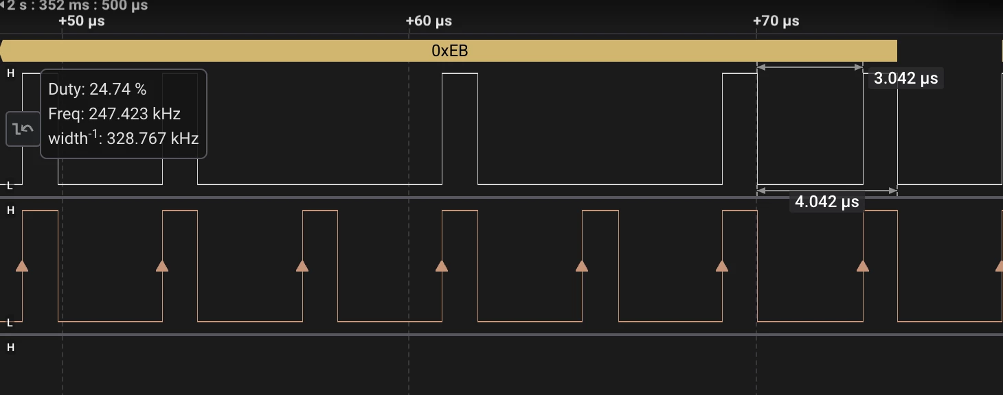
- Screenshot of the logic analyzer

Screenshot 2024-05-12 at 06.30.59.png
As you can see I do not have 3us but 3.042 and this is not always the case
 

Clock configuration
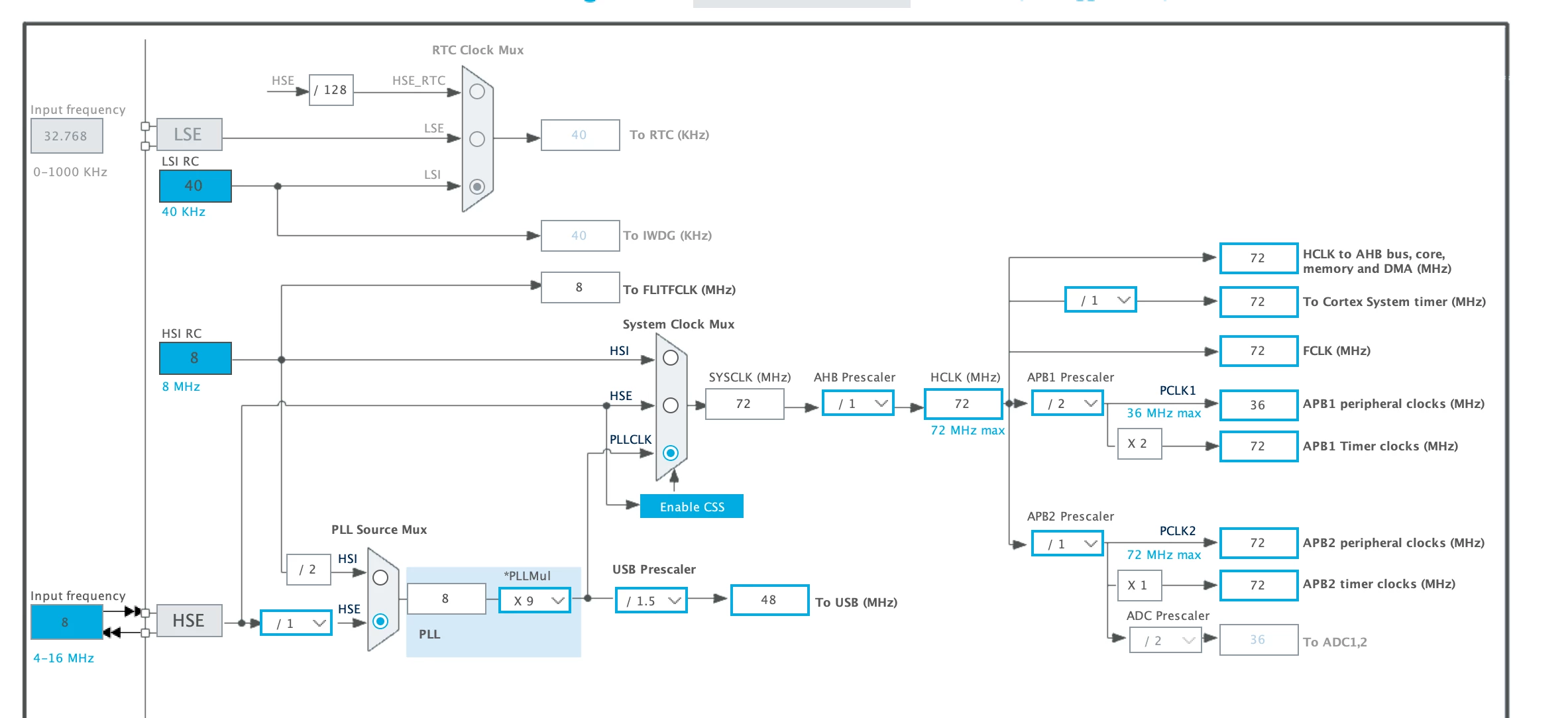
Screenshot 2024-05-12 at 06.32.34.png

Port configuration:


GPIO_InitStruct.Pin = GPIO_PIN_13| READ_PULSE_Pin|READ_CLK_Pin;
GPIO_InitStruct.Mode = GPIO_MODE_OUTPUT_PP;
GPIO_InitStruct.Pull = GPIO_NOPULL;
GPIO_InitStruct.Speed=GPIO_SPEED_FREQ_HIGH;
HAL_GPIO_Init(GPIOC, &GPIO_InitStruct);
 
Assembly code : 
 
.global wait_1us
wait_1us:
.fnstart
push {lr}
nop ;// 1 1
nop ;// 1 2
mov r2,#20 ;// 1 3
wait_1us_1:
subs r2,r2,#1 ;// 1 1
bne wait_1us_1 ;// 1 2
pop {lr}
bx lr // return from function call
.fnend

.global wait_3us
wait_3us:
.fnstart
push {lr}
nop
nop
wait_3us_1:
subs r2,r2,#1
bne wait_3us_1
pop {lr}
bx lr // return from function call
.fnend
 
 
sendByte:
 
and r5,r3,0x80000000;// 1 1
lsl r3,r3,#1 ;// 1 2 // right shift r3 by 1
subs r4,r4,#1 ;// 1 3 //; dec r4 bit counter
//mov r6,#0 // Reset the DWT Cycle counter for debug cycle counting
//ldr r6,=DWTCYCNT
//mov r2,#0
//str r2,[r6] // end
bne sendBit ;// 1 4
beq process ;// 1 5
// Clk 15, Readpulse 14, Enable 13
sendBit:
ldr r6,=PIN_BSRR ;// 2 2
LDR r2, [r6] ;// 3 5
cmp r5,#0 ;// 1 6
ITE EQ ;// 1 7

 
ORREQ r2,r2, #0x80000000 ;// 1 8 set bit 13 to 1, OR with 0000 0010 0000 0000 0x2000 (Bit13) 0x6000 (Bit13 & 14)
ORRNE r2,r2, #0x00008000 ;// 1 9 set bit 29 to 1, OR with 0010 0000 0000 0000
 
 
ORR r2,r2, #0x00004000 ;// 1 8 set bit 13 to 1, OR with 0000 0010 0000 0000 0x2000 (Bit13) 0x6000 (Bit13 & 14)
 
STR r2, [r6] ;// 1 10 set the GPIO port -> from this point we need 1us, 72 CPU cycles (to be confirmed)
bl wait_1us ;// 65 75 144 209
ORR r2,r2, #0xC0000000 ;// 1 12 ; // Bring the pin down
STR r2,[r6] ;// 1 13 ; //
; // We need to adjust the duration of the 3us function if it is the first bit (coming from process less 10 cycle)
cmp r4,#1
ite eq
moveq r2,#56
movne r2,#62
bl wait_3us ; // wait for 3 us in total
b sendByte


I do not know where to look at to be honnest

 

This topic has been closed for replies.

40 replies

Danish1
Lead III
May 12, 2024

Even something as “lowly” as stm32f1 does not guarantee cycle-by-cycle timing accuracy. Where there are things like FLASH accelarators and multiple clocks in a system, precise timing becomes unpredictable, particularly if you have other things going on such as DMA or interrupts.

(I think stm32f0 data sheets, in contrast, do mention cycle-by-cycle predictability).

You could reduce the number of things “going on” by putting your delay code inline rather than as a subroutine call - this will avoid delay-unpredictability associated with the jump and push/pull of PC to/from the stack.
How certain are you of the delay error? Are you using a Is it consistent or only on some cycles? I see you are using HSE but is it a crystal or a lower-accuracy ceramic resonator?

You do not go into why timing is so critical for your application. But if it is, you might be better off using DMA driven by a timer to pump your pre-processed pattern to the BSRR register.

vbessonAuthor
Senior
May 12, 2024

Thanks Danish1,

Timing is critical because I am interfacing an Old Apple II SDISK with a STM32 to simulate the floppy disk drive. The protocol used is a very specific data transfer protocol without clk pulse but only sequence of 1us data signal, 3us pause and so on for 402 encoded bytes (256 with encoding). I really need something very accurate. It works like a charm on a AVR ATMEGA328P.

I am new to STM32, and very surprise by the unpredictable clock approach.

I have tried the inline of the wait procedure, it helps a bit but it is not yet really accurate. 

I will try the DMA approach (even if I know nothing on ARM DMA with timer), would you have an example where I can start learning how it works ? 

Vincent

vbessonAuthor
Senior
May 12, 2024

I have checked how DMA works does it mean that I have to convert each Byte to an array of 8 uint32 and to convert to match BSSR ?

so for 402 Bytes I need a 8x402 of uint array right to feed the DMA ?

If I used circular buffer, how do I feed the buffer ? 

How do I manage 1us data pulse and 3 us pause ? another timer ? in that case how to sync the 2 timer ? 

Sorry for all this newbie question

Thanks 

Vincent


David Littell
Senior II
May 12, 2024

If your data pins are all on one port you could use a 4x402 (zeroed first!) buffer, write your encoded data in every 4th location, and use DMA metered by a 1 uSec timer to blow out the entire buffer.  Or maybe I missed a detail...  ;)

Welcome to the STM32.  There are probably some Application Notes that can help with DMA and timer setup.  And there may be something in the CubeMX examples for the F103 that might be helpful - worth a look.

vbessonAuthor
Senior
May 12, 2024

Hello David, 

thanks for your answer, I discover the power of the STM32 and I like it ;)

Very good idea to have 1 data at every 4th location, I have only 1 data pin, and it means that I need 4x8(bit)x402(Bytes) ?

Is there a way to recharge the buffer to be sent using circular ? if it make sense, how do I detect the DMA position ?

Vincent  

AScha.3
Super User
May 12, 2024

You can set the DMA to circular mode, 2 X size of your array with data, then use the half and full buffer callback to fill in new data.

So DMA write continuous data stream without interruption and you have time to fill the next buffer it will send.

If you feel a post has answered your question, please click on " Best Answer ".
vbessonAuthor
Senior
May 12, 2024

I see that there is a half transfer interrupt that I would use to update the first half of the buffer ? would that work ? 

Vincent

David Littell
Senior II
May 12, 2024

Ah, now I see (a little) more!  You're interfacing with this:

https://www.bigmessowires.com/2021/11/12/the-amazing-disk-ii-controller-card/

and

https://embeddedmicro.weebly.com/apple-2iie.html

...right?

If so, maybe instead of bit-banging it with a GPIO and DMA+timer you could use either a USART in synchronous or SPI.  Just a thought... ;)

vbessonAuthor
Senior
May 13, 2024

Yes this is my goal, I have done it with the ATMEGA328P but the SPI speed does not allow accurate writing, 

I have done a lot of trick to make it working... now I try with stm32.

My approach is:

- FatFS to select the right file, 

- Direct fat allocation reading to get the cluster / sector match

- Reading is very fast on stm32, less than 3ms to read a sector. As per the specification I have 20ms.

- Using Assembly to send bit by bit the buffer (not working), so I am testing now the approach with the DMA and the timer.

I do not get your point with USART in synchronous or SPI ? you mean having a SPI to DMA and then DMA to USART ?


Just a side question: I have the feeling that my blue pill is not with a genuine st chip (ID change). Would that impact the cycle to cycle predictability ? 

Vincent 

AScha.3
Super User
May 13, 2024

>Just a side question: I have the feeling that my blue pill is not with a genuine st chip (ID change). Would that impact the cycle to cycle predictability ? 

No , is same - because is same core.

see for the chips inside :

https://www.richis-lab.de/STM32.htm


> I have the feeling that my blue pill is not with a genuine st chip (ID change)

Whats written on chip ?

Whats its ID ?

If you feel a post has answered your question, please click on " Best Answer ".
vbessonAuthor
Senior
May 13, 2024

Ok thanks, 

I am using OpenOCD and debug works fine, 

I am implementing the DMA approach, but after that, I am kine to understand why I have a cycle or more shift with assembly code, (maybe I need to disable all interrupts)

Vincent


AScha.3
Super User
May 13, 2024

Aaaa, you cannot expect fixed timing, when INT might happen. 

Using DMA should be "better" , but still they (dma + cpu) access the same internal bus, so any access might get one or more wait states, until it gets the bus, if there is the bus busy with a transfer at that moment. 

AScha3_0-1715585114898.png


If you feel a post has answered your question, please click on " Best Answer ".
unsigned_char_array
Lead III
May 13, 2024

Have you tried running the code from RAM instead of FLASH? This might improve timing.

"Kudo posts if you have the same problem and kudo replies if the solution works.Click ""Accept as Solution"" if a reply solved your problem. If no solution was posted please answer with your own."
waclawek.jan
Super User
May 13, 2024

Forget about bit-banging, whether asm or DMA.

If you want cycle precision, just use a timer. Or SPI, or whatever other hardware is suitable.

JW

vbessonAuthor
Senior
May 13, 2024

I will try the DMA + SRAM and maybe checking interrupt as well


Vincent 

vbessonAuthor
Senior
May 13, 2024

This is the view NVIC in CubeMX,

Screenshot 2024-05-13 at 14.06.54.png

Screenshot 2024-05-13 at 14.07.11.png

Does it change something to uncheck these ?

Vincent


vbessonAuthor
Senior
May 13, 2024

This is getting really embarrassing ... ;)

Putting DMA in motion, I have better accuracy but stil some glitch... this is crazy... really really crazy

I do not understand...

V


vbessonAuthor
Senior
May 13, 2024


Frame should all be 1us High and 3us low, and I still have glitches... 

Screenshot 2024-05-13 at 21.06.47.png

unsigned_char_array
Lead III
May 13, 2024

I don't see any glitches in your screenshot.

Timing also looks good. The imperfections be an issue with synchronization between the logic analyzer and the microcontroller. Try a logic analyzer with a higher clock and you might see even better timing. Clock dither of the MCU and/or the logic analyzer can also be a factor. Rise time can also be a factor in imperfect measuring of pulse widths.

You say your logic analyzer is clocked at 24MHz, but that would make 3.063us about 73.512 clock cycles of your logic analyzer (or exactly 73.5 cycles and the 3.063 is a rounded number). So that cannot be correct. Does it sample at both edges of the clock? So 48 MSamples/second?

"Kudo posts if you have the same problem and kudo replies if the solution works.Click ""Accept as Solution"" if a reply solved your problem. If no solution was posted please answer with your own."
vbessonAuthor
Senior
May 14, 2024

I have done sampling at different logic analyser speed rate and the pulse timing is not right. I have a comparison with an ATMEGA328P. 

The issue is that I have 402 bytes per data stream to be sent, it means 402*8*4 us period = 12 864 us for a data sector. 

When I have 0.063 us shift time to time, I can have more than 1 bit or 2 shift in the end and data corruption with the 2 byte XOR CRC send at the end of the transfer.

I found an interesting article, and I am currently testing it Disabling / enabling IRQ on STM32 for atomic read 

Will keep you posted

Vincent