


What is the maximum input voltage that can be applied to my STM32 GPIO?
STM32s are typically composed of a mixture of three-volt (3V) tolerant and five-volt (5V) tolerant GPIOs. Tolerant represents the voltage value which can be accepted by the GPIO. Please be wary of each GPIO's maximum voltage tolerance, as applying more voltage than the GPIO's rated tolerance could severely damage the chip.
Some uses for 5V tolerant GPIOs include but are not limited to communicating directly with 5V buses (e.g. I2C, UART), 5V ADC conversions, and driving white LEDs. For additional application examples, please review section 5V tolerant application examples within AN4899.
We recommend planning and mapping out each GPIO’s tolerance structures to help you maximize your selected STM32 and its GPIOs’ capabilities.
In this article we will go over how to determine which GPIOs are 3V and 5V tolerant as well as go over the general "rule of thumb" to follow in terms of determining the maximum input voltage that can be applied to the GPIO when the STM32 is powered within the specifications per the part’s datasheet.
Determining the tolerance of your GPIO:
As an example, we will use the STM32G0B1CE and will be evaluating the pins PA5 and PE5.
However, as each STM32 device is unique you will need to refer to your specific STM32’s datasheet as table labeling and content could vary between different devices.
Step 1. Locate your GPIO in the pin assignment and description table within your device’s datasheet.
Using the table below, we can see that PA5 has I/O structure TT_ea: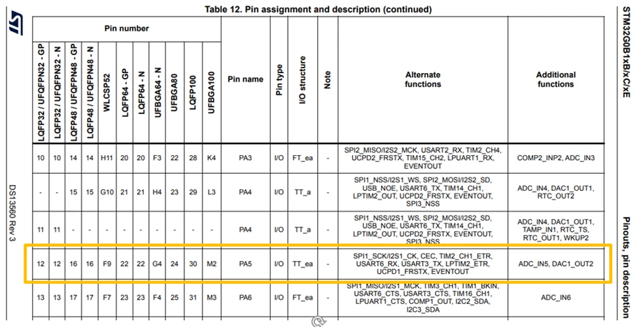
Using the table below, we can see that PE5 has the I/O structure FT: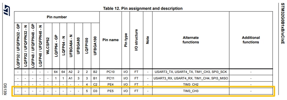
Step 2. Several GPIO structures are available across the range of STM32 devices, and each structure is associated with a list of options. You will want to locate the terms and symbols table or section within your device’s datasheet which summarizes the GPIO definitions and abbreviations applicable to STM32 products.
In the STM32G0B1’s datasheet, the legend to use to decipher the I/O’s structure in Table 11 as shown below: 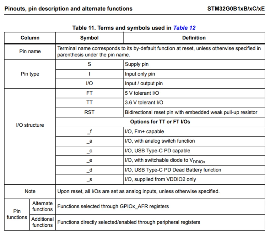
Step 3. Using the determined I/O structure in step 1 along with I/O structure legend in step 2, decipher the GPIO’s voltage tolerance and if applicable, options.
PA5’s I/O structure is TT_ea. Referring to the table in step 2, we can determine that PA5 is a 3.6V tolerant I/O with both analog switch function and switchable diode to VDDIOx.
PE5’s I/O structure is FT. Referring to the table in step 2, we can determine that PE5 is simply a 5V tolerant I/O with no additional options.
3V tolerant / compliant GPIOs (TT):
In general, the input voltage on 3V tolerant GPIOs cannot exceed VDD+0.3V. Furthermore, this holds true if the pin is used as a GPIO input or as some digital alternate function input (e.g. USART_RX).
However, if some analog input function is enabled on the GPIO (e.g. I/O’s structure is of TT_a with an ADC input active, COMP input, or an OPAMP input), the maximum voltage applied must be less than VDDA (respective of VREF+) + 0.3V. Otherwise, there will be injection into VDDA or VREF+.
The injection current is forbidden because the injection occurs inside the ADC through small parasitic diodes not capable of handling the current.
This voltage maximum information can be found in AN4899 within the 3V and 5V tolerant section: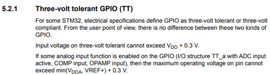
5V tolerant GPIOs (FT):
These GPIOs are tolerant to VDD + 3.6V, meaning that the I/O pins can accept such voltages without causing leakage current and damages on the GPIOs. Furthermore, this holds true if the pin is used as a GPIO input or as some digital alternate function input (e.g. USART_RX).
However, if some analog input function is enabled on the GPIO (e.g. I/O’s structure is of FT_a, FT_fa, FT_ea, etc. with an ADC input active, COMP input, or an OPAMP input), then the maximum voltage applied must be less than VDDA (respective of VREF+) + 0.3V. Otherwise, there will be injection into VDDA or VREF+. The injection current is forbidden because the injection is inside the ADC where small structures reside and injection current is limited (through small parasitic diode).
This voltage maximum information can be found in AN4899 within the 3V and 5V tolerant section: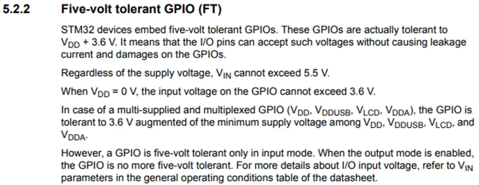
Step 4. In step 3 we concluded the following about PA5 and PE5:
PA5 is a 3.6V tolerant I/O with both analog switch function and switchable diode to VDDIOx whereas PE5 is simply a 5V tolerant I/O.
This means that my input voltage to PA5 cannot exceed VDD+0.3V. However, I must also remember that if PA5 has some analog input function enabled on it, then my input voltage must be less than VDDA (respective to VREF+) + 0.3V.
As PE5 is a simple FT (5V tolerant) pin without analog functionality, my input voltage for this GPIO can range up to VDD + 3.6V.