


Christophe VRIGNAUD
ST Employee
September 14, 2023

FAQ: STM32H7 - How to read RAMECC_MxFAR failing address

  • How to access to the right RAMECC monitor to get the RAM failing address when an ECC error occurs?
  • How to translate the content of the failing address register to the actual RAM address (e.g. FADD= 0x2004)?

Note: For simplicity and clarity, the description is based on the STM32H74x/5x series. The description would be similar for other STM32H7 series and can be found in the reference manual.
 

1. RAMECC controllers

The number of controllers depends on the STM32H7 series.
 

  • The STM32H74x/5x and STM32H72x/3x has one RAMECC controller per power domain.
    • RAMECC controller for Domain 1 (D1) = RAMECC1

    • RAMECC controller for Domain 2 (D2) = RAMECC2

    • RAMECC controller for Domain 3 (D3) = RAMECC3

​​​​​​​​​​

  • The STM32H7Ax/Bx has only one RAMECC controller.
    • RAMECC controller for the CPU Domain (CD) = RAMECC

2. RAMECC monitors

The list of monitors varies depending on the STM32H7 series.
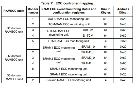
The STM32H74x/5x has one monitor for each RAM block in the MCU.

  • RAMECC1 controller has 5 monitors for D1
  • RAMECC2 controller has 5 monitors for D2
  • RAMECC3 controller has 2 monitors for D3

The detail is given in table 11 of the reference manual.
 

ChristopheVRIGNAUD_0-1694682627727.png


3. RAMECC registers address

From table 8 of the reference manual:

 
Boundary address Peripheral
0x58027000 - 0x580273FF RAMECC3
0x52009000 - 0x520093FF RAMECC1
0x48023000 - 0x480233FF RAMECC2


4. RAMECC exception vectors

From table 143 of the reference manual:

 
Signal Priority NVIC
position
Acronym Description Address offset
ramecc1_it 152 145 RAMECC1 ECC diagnostic global interrupt for RAMECC D1 0x0000 0284
ramecc2_it RAMECC2 ECC diagnostic global interrupt for RAMECC D2
ramecc3_it RAMECC3 ECC diagnostic global interrupt for RAMECC D3


5. RAMECC registers - e.g. RAMECC1

For RAMECC1, the boundary addresses are 0x52009000 - 0x520093FF (table 8 of the reference manual).
The addresses of the registers for each monitor are as follows:

  • RAMECC_IER      --  interrupt enable
=> Address offset: 0x00
=>  0x52009000
  • RAMECC_MxCR  --  configuration
=> Address offset: 0x20 * x
=> x = ECC monitoring unit number
=> 0x52009000 + 0x20 * x                  with x = [1..5]
 
=> 0x52009020   Monitor 1 -  AXI SRAM ECC monitoring unit                           512Kb
=> 0x52009040   Monitor 2 -  ITCM-RAM ECC monitoring unit                            64kB
=> 0x52009060   Monitor 3 -  DTCM-RAM ECC monitoring unit for D0TCM        64Kb
=> 0x52009080   Monitor 4 -  DTCM-RAM ECC monitoring unit for D1TCM        64Kb
=> 0x520090a0   Monitor 5 -  ETM RAM ECC monitoring unit                                4Kb


  • RAMECC_MxSR  --  status
=> Address offset: 0x24 + 0x20 * (x - 1)
=> x = ECC monitoring unit number
 
=> 0x52009000 + 0x24 + 0x20 * (x-1)   with x = [1..5]
=> 0x52009024 + 0x20 * (x-1)               with x = [1..5]
 
=> 0x52009024   Monitor 1
=> 0x52009044   Monitor 2
=> 0x52009064   Monitor 3
=> 0x52009084   Monitor 4
=> 0x520090a4   Monitor 5
 
  • RAMECC_MxFAR  --  failing address
=> Address offset: 0x28 + 0x20 * (x-1)
=> x = ECC monitoring unit number
 
=> 0x52009000 + 0x28 + 0x20 * (x-1)   with x = [1..5]
=> 0x52009028 + 0x20 * (x-1)               with x = [1..5]
 
=> 0x52009028   Monitor 1
=> 0x52009048   Monitor 2
=> 0x52009068   Monitor 3
=> 0x52009088   Monitor 4
=> 0x520090a8   Monitor 5
 
  • RAMECC_MxFDRL  --  failing data low
=> Address offset: 0x2C + 0x20 * (x-1)
=> x = ECC monitoring unit number
 
=> 0x52009000 + 0x2c + 0x20 * (x-1)   with x = [1..5]
=> 0x5200902c + 0x20 * (x-1)               with x = [1..5]
 
=> 0x5200902c   Monitor 1
=> 0x5200904c   Monitor 2
=> 0x5200906c   Monitor 3
=> 0x5200908c   Monitor 4
=> 0x520090ac   Monitor 5
 
  • RAMECC_MxFDRH  --  failing data high
=> Address offset: 0x30 + 0x20 * (x-1)
=> x = ECC monitoring unit number
 
=> 0x52009000 + 0x30 + 0x20 * (x-1)    with x = [1..5]
=> 0x52009030 + 0x20 * (x-1)                with x = [1..5]
 
=> 0x52009030   Monitor 1
=> 0x52009050   Monitor 2
=> 0x52009070   Monitor 3
=> 0x52009090   Monitor 4
=> 0x520090b0   Monitor 5
 
  • RAMECC_MxFECR  --  failing ECC error code
=> Address offset: 0x34 + 0x20 * (x-1)
=> x = ECC monitoring unit number
 
=> 0x52009000 + 0x34 + 0x20 * (x-1)   with x = [1..5]
=> 0x52009034 + 0x20 * (x-1)               with x = [1..5]
 
=> 0x52009034   Monitor 1
=> 0x52009054   Monitor 2
=> 0x52009074   Monitor 3
=> 0x52009094   Monitor 4
=> 0x520090b4   Monitor 5

6. How to get the failing address from the content of RAMECC_MxFAR

The information given by the RAMECC_MxFAR register is described in the reference manual as the failing address (FADD) for the monitor x.
 

Bits 31:0   FADD[31:0]: ECC error failing address
 When an ECC error occurs the FADD bitfield contains the address that generated the ECC error.

In fact, the address in FADD[31:0] is relative and it points to a word, not a bit. To calculate the actual RAM address, the following formula must be applied:
 
RAM Address  =  RAM memory start address  +  FADD  *  word size in byte
 

Example with FADD= 0x2004:

  • For 64-bit word size memory like AXI SRAM:

0x2400 0000 + 0x2004 * 8 = 0x2401 0020

  • For 32-bit word size memory like SRAM1:

0x3000 0000 + 0x2004 * 4 = 0x3000 8010

7. Related links

RAM ECC monitoring is described in the reference manual  -  section 3  -  RAM ECC monitoring (RAMECC).

  • RM0433 STM32H742, STM32H743/753 and STM32H750 Value line advanced Arm®-based 32-bit MCUs
  • RM0468 STM32H723/733, STM32H725/735 and STM32H730 Value line advanced Arm®-based 32-bit MCUs
  • RM0455 STM32H7A3/7B3 and STM32H7B0 Value line advanced Arm®-based 32-bit MCUs

The error correction code (ECC) management and implementation on STM32 microcontrollers is described in:

  • AN5342 How to use error correction code (ECC) management for internal memories protection on STM32 MCUs

This article was originally published 2022-06-02.
Before republication the article had 271 views.

This topic has been closed for replies.

13 replies

Christophe VRIGNAUD
ST Employee
July 12, 2024

Hi @theHolgi 

From which IDE does this screenshot come from? And which version of the tool? On which OS?
Which debugger do you use? (I've found a picture of STM32CubeIDE on MacOS with JLink displaying the SFRs in the memory view: from this I would guess that you are using JLink, right?)

I don't have this view with STM32CubeIDE version 1.16.0 and STLink-V3 debugger. I have a separate SFR registers view as shown in the picture below.

2024-07-12 19_02_02-.png There is no RAMECC_M0xx registers; it starts with RAMECC_M1xx for monitor 1.

It seems there is a shift in your view, with the values of monitor 1 displayed with the addresses of monitor 2.

Moreover, the RAMECC_M1FDRL = 0xA3837F0E. In memory, the value at @0x0000FCE0 is 0xA3837F1E, which is a bit different.
Have you verified that you don't find the content of the FDRL and FDRH registers in AXI SRAM?

Associate
August 8, 2024

Hi @Christophe VRIGNAUD ,

I am using Eclipse on Linux; the connection is with JLink so it is using JLinkGDBServer on the host side.

The SFR view is determined by the SVD file you use. The official SVD has the ECC units like you are showing, but it is missing other peripherals so I am using another SVD that I found on the internet. Should make my own best-of...
Anyway, that does not invalidate the registers' content and is why I was always citing the register addresses to remove ambiguity.

About the difference between FDR and memory view, that's actually kind of interesting since with the single ECC error that is signaled, the content should still be unambiguous even on a second reading, which the debugger connection will do.

My overall imression is that the hardware will not like multiple reads on failing memory, or follow-up errors on a different address (the memory view reads a fairly large section of uninitialized RAM), and therefore I am generous about 1 bit difference to the expected value.

I would make sure to NOT have any memory view open before you reach the fault handler and have written down the peripheral's registers, and then trust the memory view only for plausibility cross-reference.

Associate
April 23, 2025

     We had a chance to put STM32H743 under proton single event test, using ~200MeV proton beam. 
Because there is NO official documentation on how to "write back the corrected data" and offering a code example, we basically adopt the code of @theHolgi in the previous reply. We read the whole RAM except for ETMRAM, and logout the the falling address if callback triggers. In the callback, data writeback using the data contained in the RAMECC_MxFDRL/H (we suppose it is the CORRECTED data to writeback, even though it is called falling data register).  
   We have observed something really bizzare, a typical example is here:

ztliu722_0-1745391568346.png

Basically, AXI RAMECC works as expeced. However, for other RAMs, it always report the first address as failing address. Moreover, in the main loop we also check if the RAM is the same as the predefined data, in case RAMECC fails to trigger. Amazingly, the software RAM check only found two times of dismatch during the whole test. 
To sum up, if the RAMECC is working properly, it shows that except AXI RAM, all other SRAMs only fail at the initial address, even though it triggers many multiple times all at once. This is something unbelievable. We would like someone to offer a deeper explanation for this. 


Zt