Visitor II
June 19, 2026
Solved
STM32F401RET6U Custom Board Schematic Review Request
- 2 replies
- 148 views
Hello STM32 Community,
I am developing a custom board based on the STM32F302R8T6 MCU. My schematic is largely derived from the MB1136 evaluation board reference design, and I would appreciate a review from experienced STM32 users before PCB fabrication.
I would like feedback on the following areas:
- Power Supply Design
- VDD, VDDA, VBAT, VSS, and VSSA connections
- Decoupling capacitor placement and values
- Analog supply filtering
- Clock Circuit
- Main crystal oscillator connections
- 32.768 kHz RTC crystal circuit
- Load capacitor values and recommendations
- Boot and Reset Circuit
- BOOT0 configuration
- NRST pull-up and reset button circuit
- Any missing protection or filtering components
- Programming and Debugging
- SWD interface (SWDIO, SWCLK, NRST, SWO)
- Compatibility with ST-LINK
- Ability to program and debug reliably
- GPIO Connections
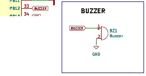
- Review of user button, status LEDs, buzzer, and external interfaces
- Any pins that should not be used for GPIO due to boot/debug functions
- General Design Review
- Any schematic mistakes or missing components
- Recommendations based on STM32 hardware design guidelines
- Potential issues that could affect flashing, debugging, startup, or long-term reliability
From my initial review:
- STM32F302R8T6 is powered from 3.3 V.
- SWD connector includes SWDIO, SWCLK, NRST, and SWO.
- BOOT0 is configured through a switch/jumper arrangement.
- External 32.768 kHz crystal is connected for RTC operation.
- Multiple decoupling capacitors are placed on VDD pins.
- SWD signals and reset are routed to the programming header.
Could you please review the schematic and let me know if there are any issues related to:
- Flashing/programming
- Power integrity
- Clock startup
- Reset/boot configuration
- STM32 hardware design best practices
Thank you for your time and support.