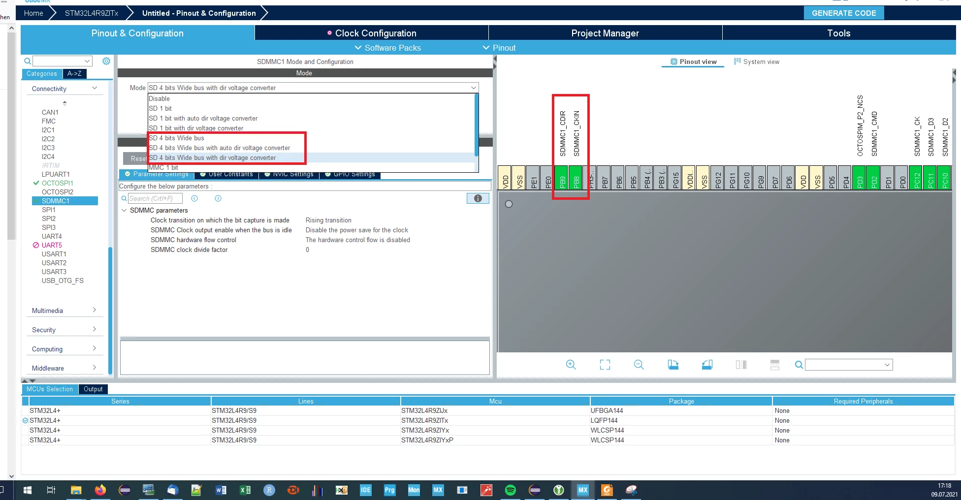
I'd imagine the reference manual has pictures, the H7 where these transceivers were first used did. Look at the H7 docs if the L4+ ones aren't illustrative.
The transceivers were use where the card voltages are dropped to support high data rates, clocks and DDR modes.
The CKIN provides a full-loop feedback to understand how the clock/data has been skewed end-to-end, allowing for correct recovery of data placed on those edges.
The direction pin controlling the buffers and it transitions through phases of the data/command transfers with the cards.
If you're driving your cards at 2.9V - 3.3V, probably should just stick to the D0..D3, CLK, CMD wiring, and SDR data clocking. Should be able to hit 50 MHz with minimal design effort.
NXP SDMMC Transceiver
The original STM32H743I-EVAL used this now obsolete IP4856CX25
https://www.nexperia.com/products/esd-protection-tvs-filtering-and-signal-conditioning/esd-protection/low-capacitance-esd-protection-for-high-speed-interfaces/IP4856CX25.html
https://www.nxp.com/products/peripherals-and-logic/voltage-level-translators/sd-3-0-sdr104-compliant-integrated-auto-direction-control-memory-card-voltage-level-translator-with-emi-filter-and-esd-protection:NVT4857UK
Not entirely on point, but good foundation
https://www.st.com/resource/en/application_note/dm00525510-getting-started-with-stm32h7-series-sdmmc-host-controller-stmicroelectronics.pdf
Tips, Buy me a coffee, or three.. PayPal Venmo (See Profile) Up vote any posts that you find helpful, it shows what's working..