Associate
June 23, 2026
Solved

Clarification on CubeMX FMC Warning for STM32H747BIT6 LQFP208

  • June 23, 2026
  • 1 reply
  • 81 views

Hello ST Team,


We are evaluating the STM32H747BIT6 in the LQFP208 package for our application. To verify the feasibility of our design, we created a CubeMX project and configured the required peripherals, including LTDC RGB888 (24-bit), FMC SDRAM (32-bit), USB FS, I2C1/I2C2/I2C3, USART1/USART3, SPI1 and TIM PWM outputs.


While configuring the project, CubeMX allowed us to assign all the required signals, and all pins are shown in green. We also checked the LTDC and FMC SDRAM signals and found that they are assigned to unique pins with no visible pin conflicts in the pinout view. Could you also review the attached .ioc file and confirm whether there are any pin conflicts that we may have overlooked?


However, CubeMX displays the following warning on the FMC peripheral

"Partly disabled conflict with:

FMC (SDRAM1): Clock and chip enable SDCKE0 + SDNE0 and/or

LTDC: Display Type RGB888 (24 bits)".


Could you please help us understand what this warning indicates and why CubeMX is reporting it? We would like to know whether this warning is expected for this configuration and if there are any specific considerations associated with it. Your clarification regarding the reason for this warning would be greatly appreciated.


For reference, we have attached the CubeMX .ioc file along with screenshots of the warning and the pin assignment view.


Thank you for your support.


Best regards,

Kannika M Mallu

Logycent

Best answer by mƎALLEm

Hello,

I did the exercise from my side by creating an ioc file from scratch:

  • Activate the SDRAM bank 1 with the same configuration as you requiring, counted the pin number used: 57 GPIOs
  • Deactivate the SDRAM and activate LTDC with the same config as your,  counted the pin number used: 28 GPIOs

The sum = 85 GPIOs

Activating both SDRAM bank 1 and LTDC interface counted the pin number and had 85 GPIOs so there is no conflict at all.

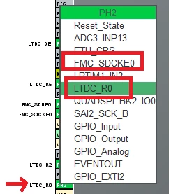
That’s just a warning and I think is about PH2 GPIO that contains the two alternate functions FMC_SDCKE0 and LTDC_R0:

And you are using different GPIOs for these two AFs.

1 reply

mƎALLEm
mƎALLEmBest answer
ST Technical Moderator
June 23, 2026

Hello,

I did the exercise from my side by creating an ioc file from scratch:

  • Activate the SDRAM bank 1 with the same configuration as you requiring, counted the pin number used: 57 GPIOs
  • Deactivate the SDRAM and activate LTDC with the same config as your,  counted the pin number used: 28 GPIOs

The sum = 85 GPIOs

Activating both SDRAM bank 1 and LTDC interface counted the pin number and had 85 GPIOs so there is no conflict at all.

That’s just a warning and I think is about PH2 GPIO that contains the two alternate functions FMC_SDCKE0 and LTDC_R0:

And you are using different GPIOs for these two AFs.

To give better visibility on the answered topics, please click "Best answer" on the reply which solved your issue or answered your question.