Query Regarding Via-on-Pad Strategy for 0.5mm pitch BGA device STM32MP157FAC1
Hello,
We are designing a custom board using the STM32MP157FAC1 device (361 balls with 0.5 mm pitch).
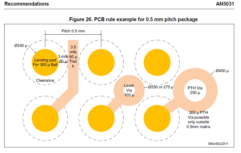
As per AN5031 (Page 50), laser vias with a 100 µm (~4 mil) drill hole diameter and 250 µm (~10 mil) outer pad diameter are recommended for BGA balls located within the 0.5 mm pitch matrix. A snapshot of the relevant section is attached for the reference.
We would like to clarify whether a Via-On-Pad strategy can be used instead of laser vias for the BGA balls within the 0.5 mm pitch matrix of STM32MP157FAC1 device.
Specifically, can we use a via of 200 µm (~8 mil) drill hole diameter and 400 µm (~16 mil) outer pad diameter as via-on-pad on the STM32MP157FAC1 BGA pads instead of the recommended laser vias ?
Kindly confirm whether this approach is acceptable from the CAD layout perspective and whether it can be used in the CAD layout of our design.
Regards,
PS