STM32WBA62 (BLE 2.4 GHz): best approach for RF matching network + PCB antenna tuning?
Context
I'm finalizing a 4-layer FR4 board with an STM32WBA62CIU6 (2.4 GHz BLE), and I'm not 100% sure about the best way to make the Bluetooth matching/tuning easier.
I first built a board with a PCB antenna identical to ST's (following the exact shape shown in application note AN5129) and a 5-element Pi network, as shown in one of the circuits in ST's application note AN5948:
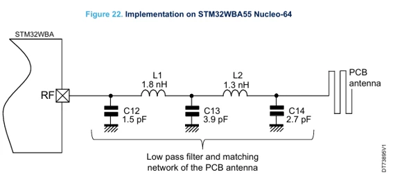
I then used a VNA, connecting at the pad where the STM32 would sit, and tuned the Pi network components so that the Pi + antenna would present an impedance of 30 + j2.5 Ω — the output impedance of my chip at 10 dBm (the power I want to use):
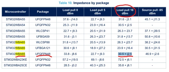
My tuning workflow was: measure with the VNA → export the result → load it into the SimSmith "Load" → place components in the simulator to get a sense of which values to use in real life. However, when I placed the real components, the result was quite different from the simulator — so different that I ended up unable to complete the tuning.
Current setup / measurements
- Stackup: 4-layer FR4. RF microstrip on Top Layer referenced to Layer 1 (inner ground), separation = prepreg PP-021, h = 0.1855 mm, bulk Dk = 4.74. Measured trace delay ≈ 6.07 ps/mm → microstrip ε_eff ≈ 3.3, VF ≈ 0.55. Trace 0.4 mm wide → Z0 ≈ 38 Ω (Altium field solver, uncontrolled).
- Measurement: R&S FSH VNA with a U.FL pigtail < 50 mm. I'm seeing common-mode / cable-position sensitivity, and my discrete-model predictions in SimSmith don't track the board well after each component change (component parasitics at 2.4 GHz).
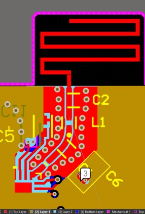
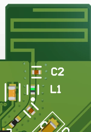
Here is the actual PCB:
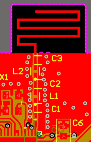
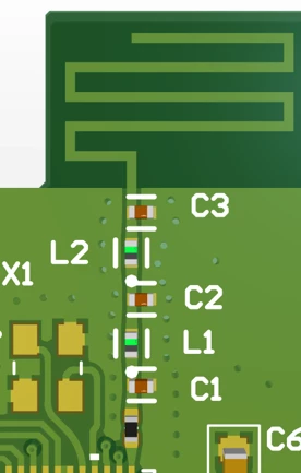
Planned changes for the next revision
For the next PCB revision I'm considering:
- Trace reference: cutting away the nearest ground plane and using the next ground layer as the reference, so I can route a wider trace with a properly calculated 50 Ω.
- Antenna: making it slightly longer so I can trim it to better tune the resistive part of the impedance.
- External antenna: adding a variant with a U.FL connector for an external antenna, to compare range.
- Matching network: building the Pi network in one of these ways:
Option 1 — a simple 3-element matching network:
Option 2 — using the MLPF-WB-04D3 (ST integrated 2.4 GHz low-pass filter) or another filter together with a Pi network. I'm not sure whether to use a Pi both before and after the filter, or just one after it.
Option 3 — a "split" approach: a 3-element Pi to bring the chip + components to 50 Ω (measured with a spectrum analyzer) and another Pi to bring the antenna to 50 Ω (measured with a VNA), with a 0 Ω resistor separating the two halves.
Questions
- Are these good ways to build this kind of PCB?
- Should I really measure the chip output with a spectrum analyzer to tune it as well, or can I trust the output impedance that ST gives in the datasheet table?