Associate III
Jan 19, 2026 11:59 AM UTC
Solved

STM32WBA5MMGH6TR Debug interface PCB layout

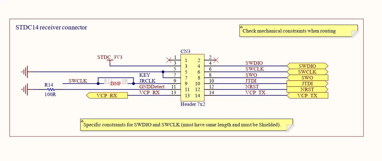
I am using STM32WBA5MMG in my design. This the development board schematic. Below image is from development board schematic.
Hariom_1-1768823941790.png

As per the constrains , SWDIO and SWCLK must be length matched. Also need to provide a shield.My questions are given below.

  1. SWDIO and SWCLK are not differential lines, why length matching is required for them.
  2. By shield did they mean routing SWDIO and SWCLK on top of a solid GND plane

Andrew Neil
Andrew NeilBest answer
Super User
Jan 19, 2026 12:19 PM UTC

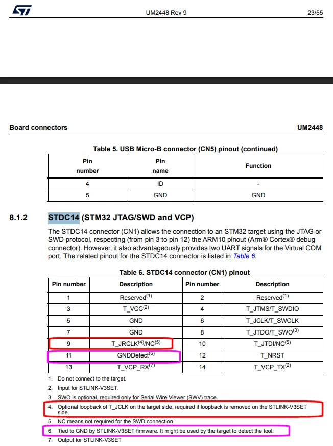
I found a description of these in the STLINK-V3SET User Manual:

AndrewNeil_1-1768825064221.png

https://www.st.com/resource/en/user_manual/um2448-stlinkv3set-debuggerprogrammer-for-stm8-and-stm32-stmicroelectronics.pdf#page=24


A complex system that works is invariably found to have evolved from a simple system that worked.A complex system designed from scratch never works and cannot be patched up to make it work.

3 replies

Andrew Neil
Super User
Jan 19, 2026 12:05 PM UTC

These are not usual requirements for SWD !

A complex system that works is invariably found to have evolved from a simple system that worked.A complex system designed from scratch never works and cannot be patched up to make it work.
HariomAuthor
Associate III
Jan 19, 2026 12:06 PM UTC

May I know what you mean by GNDDetect and KEY JRCLK signal?

Andrew Neil
Andrew NeilBest answer
Super User
Jan 19, 2026 12:19 PM UTC
A complex system that works is invariably found to have evolved from a simple system that worked.A complex system designed from scratch never works and cannot be patched up to make it work.