Solved
STM32WB55C Based BLE module design verification
Hi Team,
Am designing a BLE module using STM32WB55CEU6 for an IoT audio streaming project. Can somebody please help me in verifying the RF portion of schematics and layout. We are using an IPEX connector on board for BLE antenna and the signal is connected as below from MCU to antenna connector. Is it fine?
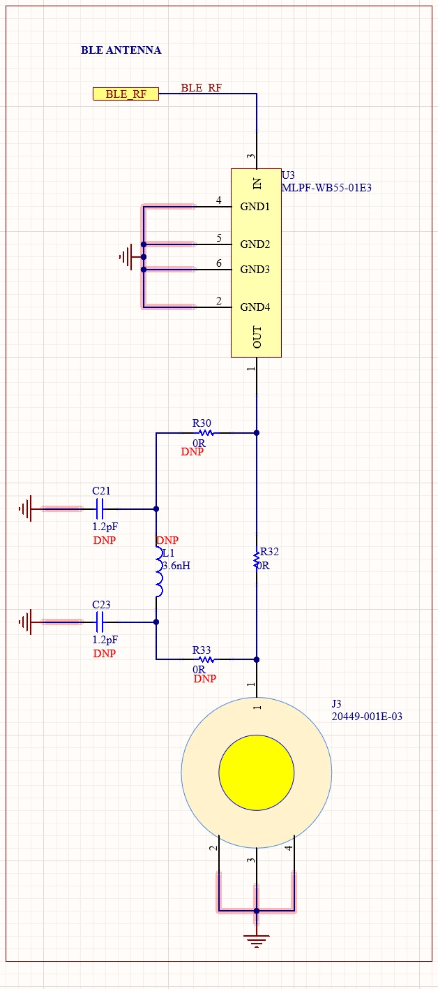
Also, I have referred layout design for dev board using the STM32WBB55 MCU and I found that for RF section there is no reference given in immediate layer ie: layer 2 for signal routed in layer 1. Whereas GND plane if given under RF section in layer 3 & 4. Even we are using a 4-Layer stack up so is it mandatory to follow same.?
Best Regards,
Vyshnav Krishnan