Solved
STM32WB10CC RF output stage design question
Hello,
For a personal project, I am designing a device that receives GPS data and transmits the UTC time information to other devices over BLE. I will also be designing a device that receives the data and displays it. For this, I have chosen the STM32WB10 MCU. I think I have a surface-level knowledge of RF, but I couldn't understand this application schematic in AN5290, page 10:
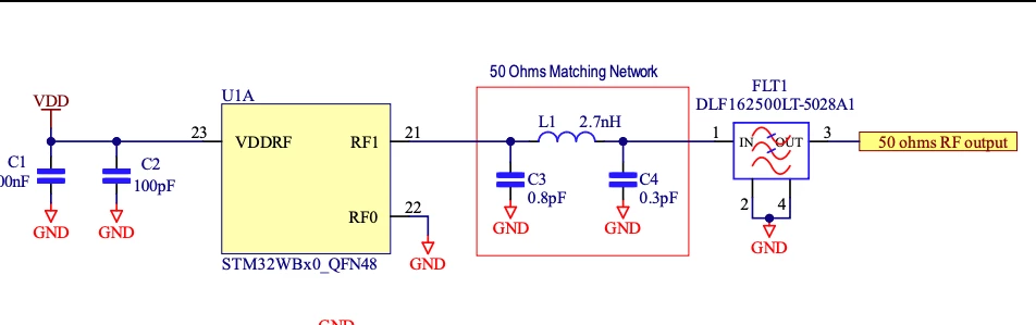
What I am confused about is the low pass filter at the end. Assuming I connect an antenna to the RF output, how would this device work in RX mode? Perhaps as a result to my inexperience with RF, the antenna being connected to the output of the LPF doesn't make sense to me. The same circuit is also showed in AN5165, page 13.
Thank you in advance for the advice.