Solved
STM32WB10 PCB Antenna from AN5129 on Custom Board
Hi everybody,
I want to design a custom PB for the STM32WB10 with the PCB antenna design from AN5129. As described in the document there is a keep out area for the antenna where no GND plane should be placed. My question about this:
If I keep this space free for the antenna, can I place components with a GND plane outside without having a cut in PCB? Or is there any interference if I do this?
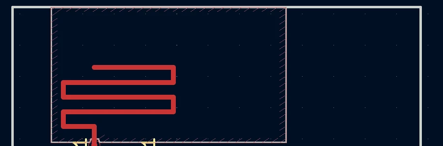
The picture shows my antenna with keep out area and I want to place something left and right to this area.