
How I Program the CPU2 memory area using STM32CubeProgrammer?
I'm trying to understand how I program the BLE Stack and FUS in the CPU2 of STM32WB55G (1Mb). When I use the binary available of ST repositoy, in default mode I program the "stm32wb5x_BLE_Stack_full_fw.bin" in address started 0x08000000, but in the release_note that is available of ST repository, it's show us that the binary needs program in address started 0x080D0000:
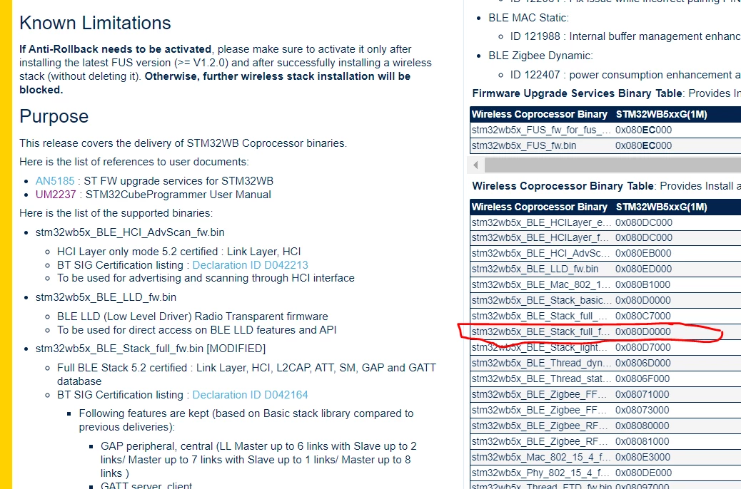
When I program with this configuration and also program the "BLE_Ota", the application works (I can see the device in the app "ST BLE SENSOR"). But I didn't understand like it works, because the BLE_Ota start address in the 0x08000000 and it's overwrite the program previous (stm32wb5x_BLE_Stack_full_fw.bin), right?
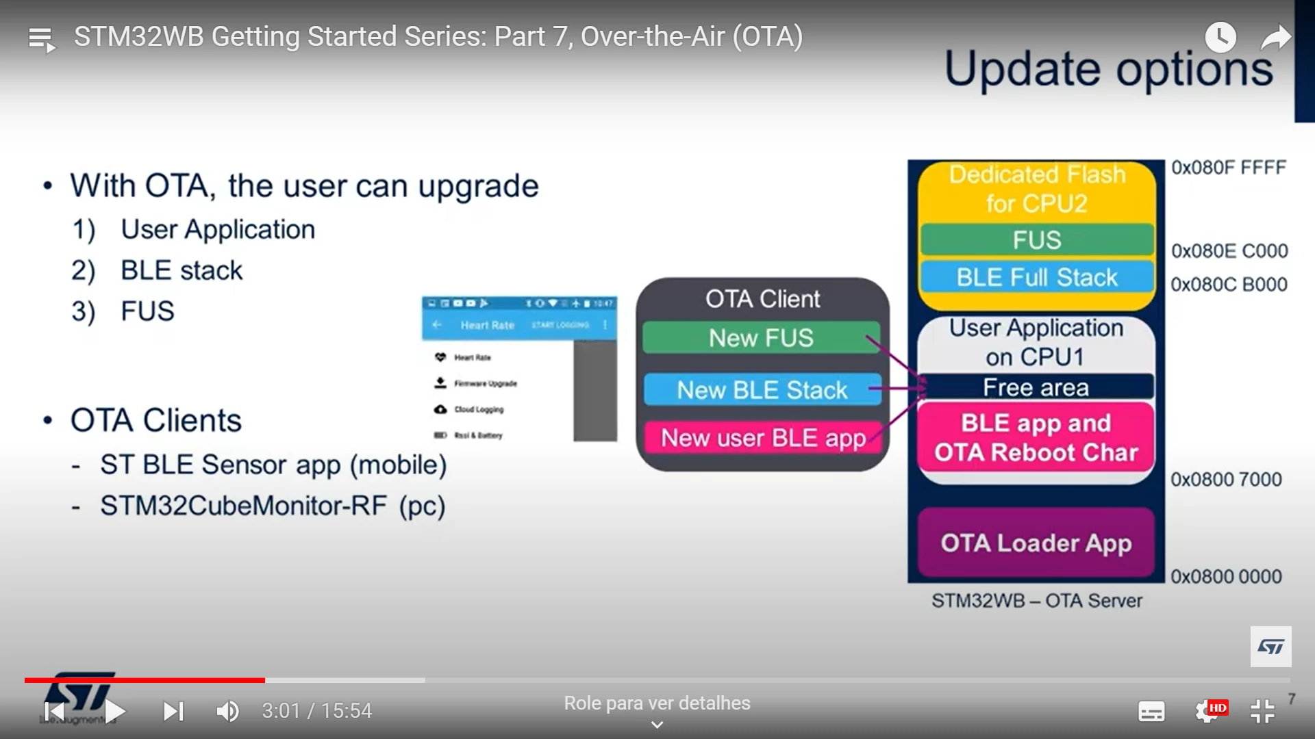
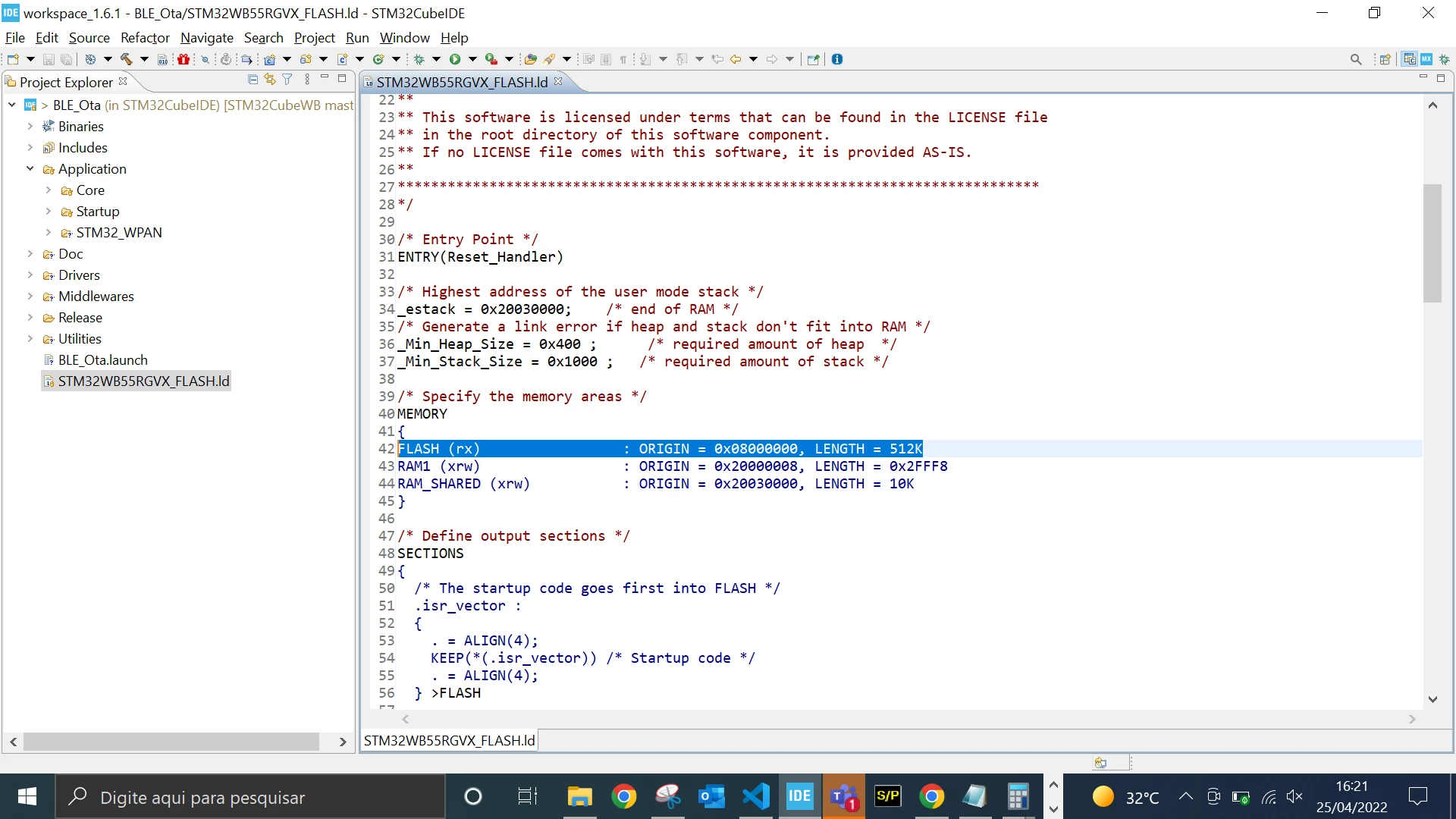 I did any tests: I Followed the video "STM32WB Getting Started Series: Part 7, Over-the-Air (OTA)" for understand the construction of memory, I understood that the memory of CPU 1 is 0x0800000 until 0x080CB000 and CPU 2 is 0x080CB000 until 0x080FFFFF:
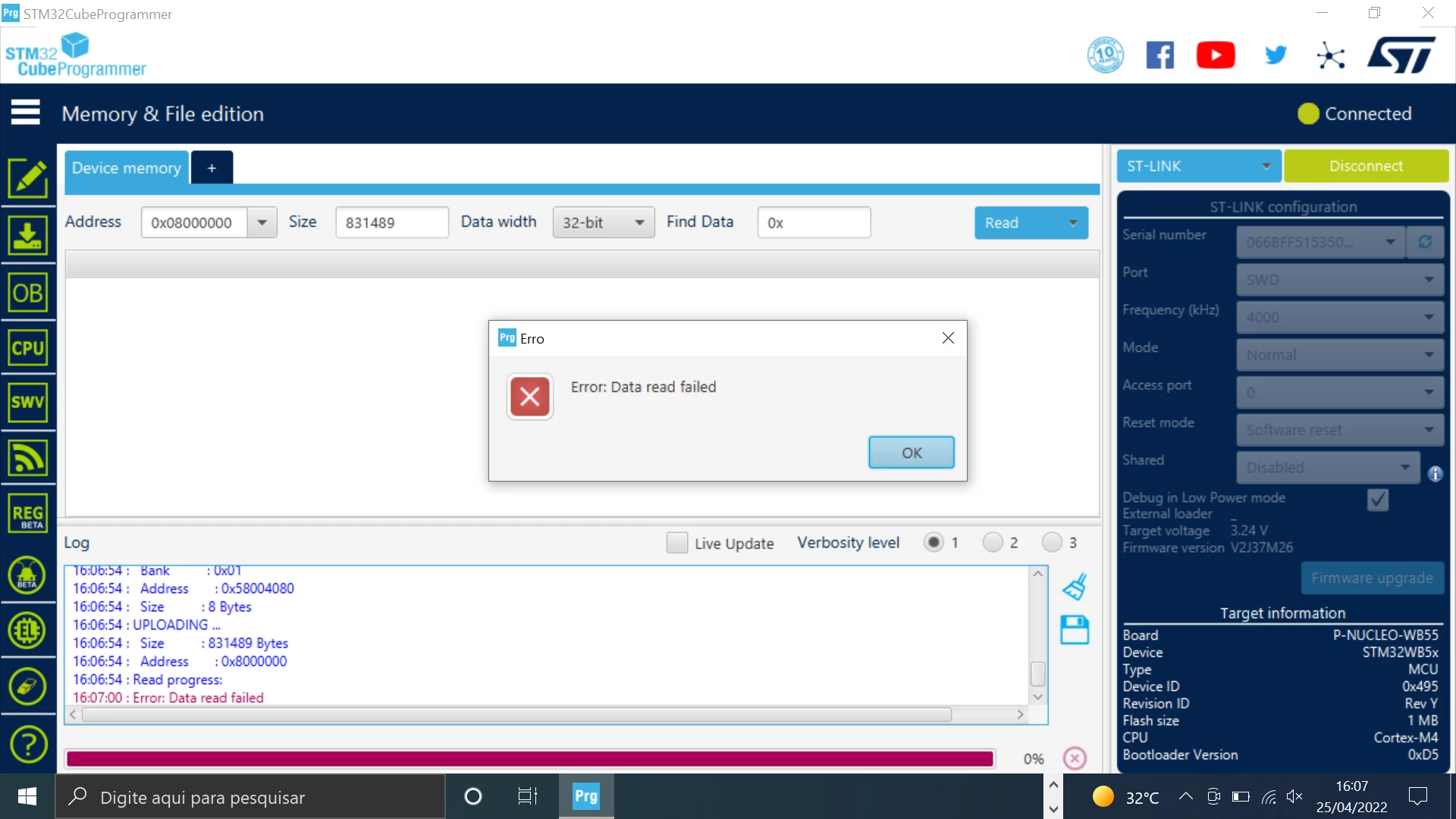
 So, when I try to read the memory of 0x080CB000, I get this message in STM32CubeProgrammer:
 But, if I try read one byte less, it's works:
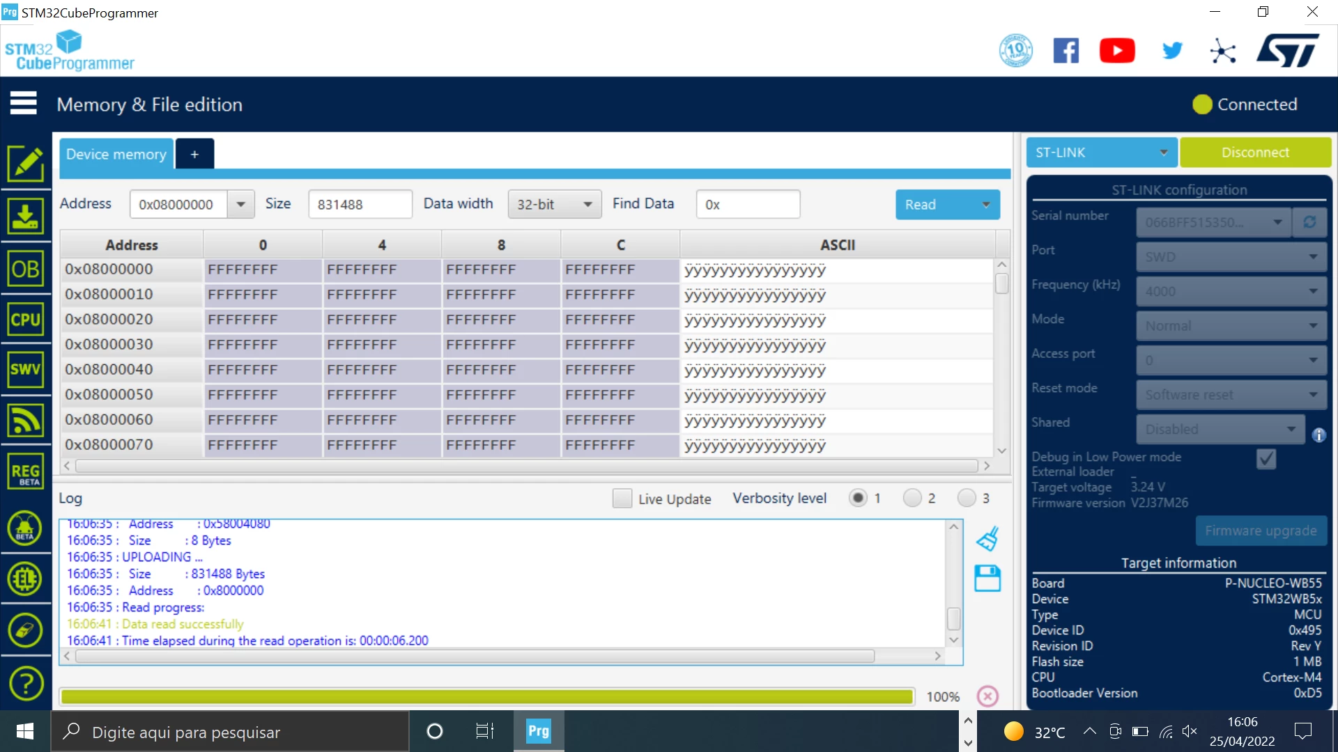 With these tests, I can understand that the STM32CubeProgrammer cannot read CPU 2. How did the firmware "stm32wb5x_BLE_Stack_full_fw.bin" go to CPU 2 and did the application work? How do I read or write to CPU 2 by STM32CubeProgrammer?