

IHarg.1
Associate II
March 5, 2024
Question

AD5129 - meander design for STM32WB Series Layer Stack Double Check

  • March 5, 2024
  • 3 replies
  • 2171 views

Hello,

I am developing a custom board with the STM32WB55RGV6 Chip and an on-board PCB antenna. The document is for a 2-layer PCB and I am needing to do a 4-layer PCB. I don't completely have the recommended stack-up, but altium shows its very close to 50Ohms. Will this work?
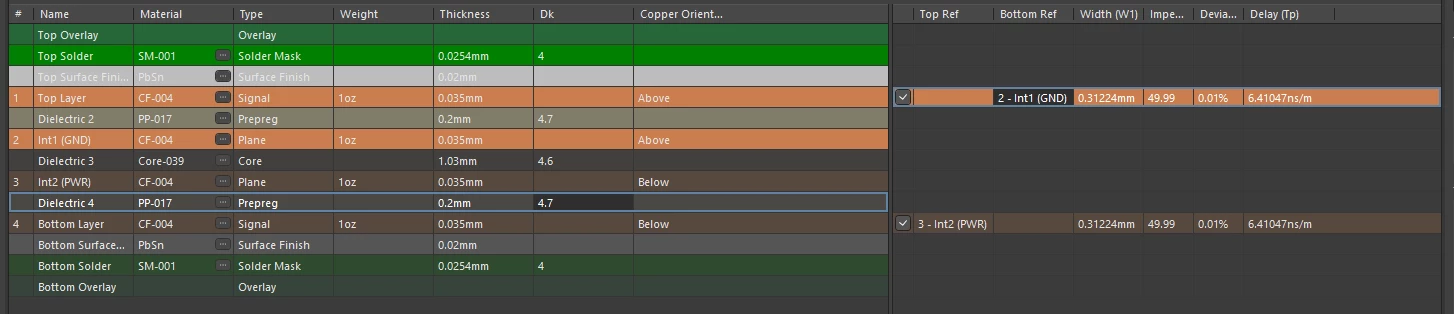

IHarg1_0-1709669410692.png

IHarg1_1-1709669456593.png


This topic has been closed for replies.

3 replies

IHarg.1
IHarg.1Author
Associate II
March 5, 2024

IHarg1_0-1709674323433.png

Here is the RF routed. Please advise if you see anything needing corrected.

IHarg.1
IHarg.1Author
Associate II
March 5, 2024

I just beefed the RF traces up to 15mils--other than the antenna which is to spec--, do I need to be more specific for impedance matching?

Remi QUINTIN
ST Technical Moderator
March 27, 2024

You may have a look at applications notes AN5290 and AN5165 where you can find information on Table 4. 4-layer PCB and on the matching network.
