What is NVSTATE in RM0481 rev 4?
In RM0481 rev 4 April 2025 I find the following text:
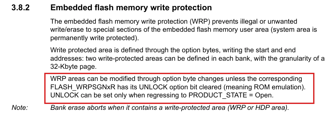
7.6.8 Write protection
A write-protected group of sectors cannot be erased nor programmed. As a result, a bank
erase cannot be performed if one group of sectors is write-protected, unless a NVSTATE
transition to OPEN is triggered (erasing the whole user flash memory).
It is not clear what NVSTATE is in this context. Is this a left-over from documentation of a different MCU?
I don’t think it is PRODUCT_STATE. Because to my understanding you can have a PRODUCT_STATE > OPEN and not enable TrustZone and then write to FLASH_WRP1R_PRG to turn off write protection - you should be able to do a bank erase on bank 1. You can set initial values with an OB but I can’t see any documentation that this also makes changing FLASH_WRP1R_PRG illegal and the relevant OBs are not protected by PRODUCT_STATE the same way as e.g. SECWM and HDP.
Same reasoning for flash bank 2.
And if you enable TrustZone, it is stated that FLASH_WRP[1, 2]R_PRG is non-secure. So as long as you don’t set part of the flash to secure watermarked, bank erase should work.
Also note that a AFAIK a regression of PRODUCT_STATE do not restore the WRP OBs to their default state.
The only other place NVSTATE is mentioned in RM0481 is in Table 507 TAMP interconnection:
tamp_itamp6 JTAG/SWD access when NVSTATE ? OPEN
Here, “NVSATE” should be “PRODUCT_STATE”?
Best regards, Jesper