Associate II
Oct 29, 2026 6:22 AM UTC
Question

What is the architecture of the differential ADC in STM32H750?

Basic SAR ADC is depicted here:
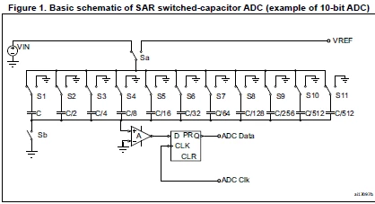
From AN2834, How to optimize the ADC ...

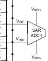
STM32H750 showed it’s ADC block:

Fig 138. from reference manual RM0433

I want to know what is inside this block? Why it’s input signal should biased to 1.65+-10% strictly? But It’s sigle ended arrangement which is simply connect the negative pin to gnd have large common mode input from 0 to Vcc?

2 replies

AScha.3
Super User
Oct 29, 2026 1:18 PM UTC

First : I am not STM , just a user of some chips.


In diff mode the signal can be :


As we dont know, whats inside the ADC , just imagine: how would I build it ?

Ok, same timing as usual, so only the input circuit could be different : most simple solution -- >

a: have the input sampling cap switched to the now “differential” called +/- inputs.

b: have a same sized cap switched to vref + and - . 

c: for conversion , switch both caps together, then convert.

Now ADC “sees” its sampling cap charged to 0...vref , if diff.in was a voltage from -vref ...vref. (-vref || + vref = 0; vref || vref = vref. ( || = parallel switched) )

This is the “trick” , because the ADC can only convert between vref- and vref+  , and adding the charged cap of same size brings the voltage in this range, no matter, the diff-input was pos or neg in voltage.

Now why this strange CMR of only +/- 10% around vref/2 ?

I assume, this is just some restriction, coming from the properties of the analog switches, as on this level of resolution (16b at 3V -- > about 45 uV  !! ) the impedance of all involved switches has to be extremely good matched and as these analog switches usually change their impedance with applied voltage , its the obvious way to have all voltages at the switches as symmetrical as possible. 

So the diff.input voltages have to be centered around mid of vref- and + , to give best performance.

If using the ADC in diff-mode you need an opamp circuit that makes the input to the ADC pins differential , but keeping its sum  always at vref/2 . The errors of the analog switches thus almost cancel each other out. Thats it.

If you feel a post has answered your question, please click on " Best Answer ".
TDK
Oct 29, 2026 3:29 PM UTC

I suspect this has more to do with ensuring ADC accuracy that with any underlying hardware limitation. If your common mode is not VREF/2, you will still get a result.

In any case, connecting the negative side to ground makes no sense. If you want a measurement relative to ground use single ended mode.

"If you feel a post has answered your question, please click ""Accept as Solution""."