

HDaji.1
Senior
November 2, 2021
Solved

Unexpected Gain in OPAMP_PGA in G431

I am testing Examples/OPAMP/OPAMP_PGA/ in G4 package code, only to find the gain is not consistent as showed below:
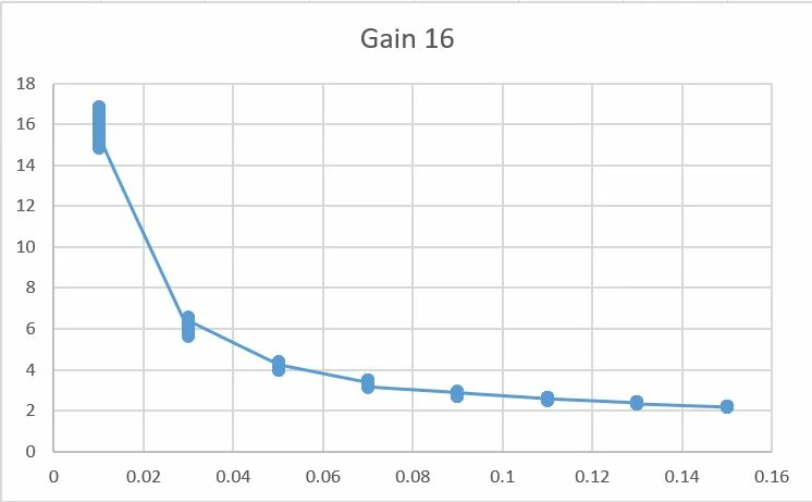
0693W00000GWAeJQAX.jpgThe OPAMP input values are 0.01,0.03, ..., 0.15, and gain is 16.

However, I measured output at ADC side, the gain drops significant as input values increase.

What went wrong?

This topic has been closed for replies.
Igor Cesko
Igor CeskoBest answer
ST Employee
November 10, 2021

Hi HDaji.1 ,

I have verified the example "OPAMP_PGA" - with small modification to input values (not sinewave waveform used in RAM but DC voltage in RAM). I used OPAMP input voltages (DAC output to OPAMP input) below 120mV to not overload the OPAMP output (120mV * gain16 = 1.92V). I have tested gains 2 .. 16 and all gains are correct.

I have tested voltages from DAC: 120mV and 12mV. For 12mV I have tested also gains 32 and 64. All gains are correct. I have measured OPAMP input and output voltages by multimeter. I have used DAC without output buffer to be able to reach such low voltages on DAC output (because DAC with buffer is not rail to rail). From measurement I determined that the OPAMP offset is about -1.5mV (no offset calibration used). This offset influences a bit the output voltage (because gain amplifies also offset) - because offset is added into input voltage.

Please measure in your configuration OPAMP input and output by multimeter/voltmeter - to determine exactly the correct gain values (oscilloscope is not precise for such low voltage measurement). If gains are correct then the problem is in ADC sampling the OPAMP output. Minimum sampling tine for OPAMP output is (according datasheet) 200ns.

Regards

Igor

20 replies

TDK
November 2, 2021

How is the output connected and how are you measuring it?

"If you feel a post has answered your question, please click ""Accept as Solution""."
HDaji.1
HDaji.1Author
Senior
November 3, 2021

I connect a DAC voltage source to PA1 (OPAMP3_VINP), and OPAMP output pin PB1 to ADC input pin PC0.

The voltage source has been verified with scope and ADC readings separately without any problem.

waclawek.jan
Super User
November 3, 2021

Maybe overloaded opamp output. Is there anything connected to it? Do the ADC readings match measured voltage? Try increasing ADC sampling time.

JW

HDaji.1
HDaji.1Author
Senior
November 6, 2021

My ADC sampling time is ADC_SAMPLETIME_2CYCLES_5, which I guess is the fastest already, isn't it?

HDaji.1
HDaji.1Author
Senior
November 6, 2021

There is no load connected to opamp output pin, other than ADC input pin.

Piranha
Principal III
November 6, 2021

> Try increasing ADC sampling time.

> is the fastest already

Read and rethink again...

HDaji.1
HDaji.1Author
Senior
November 8, 2021

changing sampling time does not help.

Igor Cesko
Igor CeskoBest answer
ST Employee
November 10, 2021

Hi HDaji.1 ,

I have verified the example "OPAMP_PGA" - with small modification to input values (not sinewave waveform used in RAM but DC voltage in RAM). I used OPAMP input voltages (DAC output to OPAMP input) below 120mV to not overload the OPAMP output (120mV * gain16 = 1.92V). I have tested gains 2 .. 16 and all gains are correct.

I have tested voltages from DAC: 120mV and 12mV. For 12mV I have tested also gains 32 and 64. All gains are correct. I have measured OPAMP input and output voltages by multimeter. I have used DAC without output buffer to be able to reach such low voltages on DAC output (because DAC with buffer is not rail to rail). From measurement I determined that the OPAMP offset is about -1.5mV (no offset calibration used). This offset influences a bit the output voltage (because gain amplifies also offset) - because offset is added into input voltage.

Please measure in your configuration OPAMP input and output by multimeter/voltmeter - to determine exactly the correct gain values (oscilloscope is not precise for such low voltage measurement). If gains are correct then the problem is in ADC sampling the OPAMP output. Minimum sampling tine for OPAMP output is (according datasheet) 200ns.

Regards

Igor

HDaji.1
HDaji.1Author
Senior
November 11, 2021

Hi Igor,

thank you very much for your effort. Much appreciate it.

In fact, my test setup is a bit complicated: I use a G4 board SPI to control a DAC board and adjust its voltage output, which is connected to the same G4 board's OPAMP input. I link OPAMP output to an ADC input channel. That's how I got the above weird result.

In the past days, I did another test: use one G4 board to control the DAC; use another G4 board's OPAMP+ADC just to read DAC output. The result looks reasonable except that when DAC output goes low as 10mV, gain is slightly higher than expected. I guess it may be caused by that OPAMP offset.

The weird result in my first attempt is caused by the test setup: too many wires.

I will try to reduce wiring as much as possible. Any other advice on how to do a decent setup for my complicated testbed?

One more question: have you tried to measure the OPAMP output using ADC input channel of the same chip or board? I wonder how big the ADC error can reach. My project requirement is to use OPAMP+ADC to read voltage in range 10~30mv, ADC reading error < 1mV after gain.

Igor Cesko
ST Employee
November 11, 2021

Hi HDaji.1 ,

This OPAMP - ADC configuration was tested. The ADC measures what is on OPAMP output (if correct minimum sampling time was applied). So the accuracy of voltage measurement is given by ADC parameters - as shown in datasheet.

This means : Total unadjusted error = 5.5LSB (datasheet data). If VREF=3.3V then 1LSB = 3.3/4095 = 0.8mV . So Total unadjusted error = 5.5 * 0.8mV = 4.4mV.

If we measure such low voltages then error will be much better - dominant is ADC offset error (gain error is not so important) then: offset error = 2.5LSB => 2mV.

Regards

Igor

HDaji.1
HDaji.1Author
Senior
November 17, 2021

Is there any way to adjust ADC error to 1LSB?

Igor Cesko
ST Employee
November 12, 2021

Hi HDaji.1,

Do not use sample and hold mode for the DAC. Modify the example in the STM32CubeMX - this is the easiest way to modify the project (*.ioc file in the example is the file for STM32CubeMX). In STM32CubeMX change the DAC mode and build the example again.

Regards

Igor

HDaji.1
HDaji.1Author
Senior
November 12, 2021

You mean this one0693W00000GXOluQAH.jpgand this one

sConfig.DAC_OutputBuffer = DAC_OUTPUTBUFFER_DISABLE;

 BTW, I am using CubeIDE not CubeMX

Igor Cesko
ST Employee
November 15, 2021

Hi HDaji.1 ,

Mode should be "Connected to external pin only".

And "Sample And Hold" should be "Sampleandhold Disable" :

0693W00000GXYX4QAP.png Regards

Igor
