Understanding SPI on the STM32F3
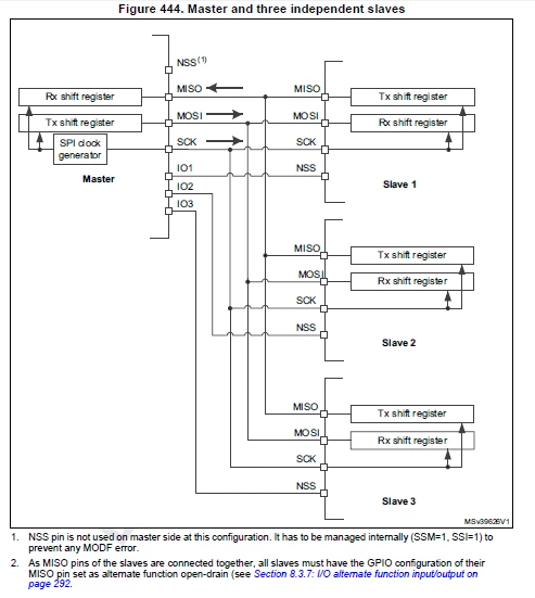
Hi, I have a NUCLEO-F303 board which I would like to use to communicate to two devices using SPI. The NUCLEO would be sending and receiving data to and from the devices via MOSI and MISO.
Looking through the datasheet, I'm very confused by the slave select management bits (SSM and SSI) under master mode, and how I should configure them for my application so that I can manually drive a GPIO pin low for slave select and then clock in/out the data.
Since I have multiple slaves, I'm assuming SSM = 1? On page 964 of the reference manual, it also says '... slave select information is driven internally by the SSI bit value in the register SPIx_CR1...'. So going by that, after I pull a GPIO chip select pin LOW, I also set SSI low to indicate that a slave has been selected? When I tried doing this, I get a frame error in the status register. I also tried leaving the SSI bit high, but the contents of the data register always reads 0xFFFF.
Any clarifications would be greatly appreciated! Thanks!
Below is my code for SPI:
// Configures GPIOA pins to use SPI1
// PB3 - SPI1_CLK (AF5)// PB4 - SPI1_MISO (AF5)// PB5 - SPI1_MOSI (AF5)void SPI1_Init(void){ uint8_t ch; if(RCC->APB2ENR & RCC_APB2ENR_SPI1EN) // SPI1 already enabled { return; } // Disable SPI while(SPI1->SR & SPI_SR_FTLVL); // Wait until no more data to transmit while(SPI1->SR & SPI_SR_BSY); // Wait until SPI is not busy SPI1->CR1 &= ~SPI_CR1_SPE; // Disable SPI1 peripheral while(SPI1->SR & SPI_SR_FRLVL) // Read all data deceived { if(SPI1->SR & SPI_SR_RXNE) { ch = SPI1->DR; } } // Initializae GPIOA and GPIOB peripheral clocks GPIOAClock(1); GPIOBClock(1); // Set PB1 and PA12 as outputs // PB1 - DAC Chip select // PA12 - BLE Chip Select GPIOA->MODER &= ~GPIO_MODER_MODER12; GPIOA->MODER |= GPIO_MODER_MODER12_0; // PA12 - Output GPIOA->OTYPER &= ~GPIO_OTYPER_OT_12; // Push pull GPIOB->MODER &= ~GPIO_MODER_MODER1; GPIOB->MODER |= GPIO_MODER_MODER1_0; // PB1 - Output GPIOB->OTYPER &= ~GPIO_OTYPER_OT_1; // Push pull GPIOA->ODR |= GPIO_ODR_12; // Set PA12 high GPIOB->ODR |= GPIO_ODR_1; // Set PB1 high // Enable SPI1 Clock RCC->APB2ENR |= RCC_APB2ENR_SPI1EN; // First, configure GPIO port to for SPI use // ====================================================== // Configure PB3, PB4, PB5 to be alternate function pins GPIOB->MODER &= ~(GPIO_MODER_MODER3 | GPIO_MODER_MODER4 | GPIO_MODER_MODER5); GPIOB->MODER |= GPIO_MODER_MODER3_1 | GPIO_MODER_MODER4_1 | GPIO_MODER_MODER5_1; // Output type as Push-pull GPIOB->OTYPER &= ~(GPIO_OTYPER_OT_3 | GPIO_OTYPER_OT_4 | GPIO_OTYPER_OT_5); // High speed for PB3, PB4, PB5 GPIOB->OSPEEDR &= ~(GPIO_OSPEEDER_OSPEEDR3 | GPIO_OSPEEDER_OSPEEDR4 | GPIO_OSPEEDER_OSPEEDR5); GPIOB->OSPEEDR |= GPIO_OSPEEDER_OSPEEDR3 | GPIO_OSPEEDER_OSPEEDR4 | GPIO_OSPEEDER_OSPEEDR5; // No pull up or pull down for CLK, MOSI. Pull up for MISO GPIOB->PUPDR &= ~(GPIO_PUPDR_PUPDR3 | GPIO_PUPDR_PUPDR4 | GPIO_PUPDR_PUPDR5); GPIOB->PUPDR |= GPIO_PUPDR_PUPDR4_0; // Set alternative function to AF5 (SPI Mode) GPIOB->AFR[0] &= ~(GPIO_AFRL_AFRL3 | GPIO_AFRL_AFRL4 | GPIO_AFRL_AFRL5); GPIOB->AFR[0] |= ( (5U << 12) | (5U << 16) | (5U << 20));// Now configure SPI settings:
SPI1->CR1 = 0x00; // Reset SPI CR1 SPI1->CR2 = 0x0700; // Reset SPI CR2: Default settings for CR2 okay for use SPI1->CR1 |= SPI_CR1_BR_0; // Spi Clock is 8 MHz / 4 = 2 MHz SPI1->CR1 &= ~(SPI_CR1_CPOL | SPI_CR1_CPHA); SPI1->CR1 &= ~SPI_CR1_RXONLY; // Full duplex mode SPI1->CR1 &= ~SPI_CR1_BIDIMODE; // 2-line unidirectional data SPI1->CR1 |= SPI_CR1_BIDIOE; // Output enabled MOSI pin SPI1->CR1 &= ~SPI_CR1_LSBFIRST; // MSB First SPI1->CR1 |= SPI_CR1_SSM; // Enable software slave management SPI1->CR1 |= SPI_CR1_MSTR; // Master Configuration SPI1->CR1 |= SPI_CR1_SSI; // Set SSI High SPI1->CR2 |= SPI_CR2_FRXTH; // Reception threshold >= 8-bits}
// Sends a single byte of data out SPI1
void SPI1_WriteByte(uint8_t data){SPI1->CR1 |= SPI_CR1_SPE; // Enable SPE
while(SPI1->SR & SPI_SR_BSY); // Wait until bus is not busy SPI1->DR = data; // write data while(!(SPI1->SR & SPI_SR_TXE)); SPI1->CR1 &= ~SPI_CR1_SPE; // Disable SPE}// Writes a string of bytes to the selected chip
void SPI1_WriteString(SPI_CHIPS chipSelect, uint8_t *s){ // Pull appropriate chip select line LOW to start transfer if(chipSelect == BLE) { GPIOA->ODR &= ~GPIO_ODR_12; } else if (chipSelect == DAC_MCP4821) { GPIOB->ODR &= ~GPIO_ODR_1; } else if (chipSelect == DAC_MCP4921) { GPIOB->ODR &= ~GPIO_ODR_1; } while(*s) { SPI1_WriteByte(*s++); } // Pull appropriate chip line HIGH to end transfer if(chipSelect == BLE) { GPIOA->ODR |= GPIO_ODR_12; } else if (chipSelect == DAC_MCP4821) { GPIOB->ODR |= GPIO_ODR_1; } else if (chipSelect == DAC_MCP4921) { GPIOB->ODR |= GPIO_ODR_1; } #nucleo-f303 #spi #stm32f3