Aurelien Robert
Associate III
August 31, 2023
Question

Understanding QSPI memory transaction timings with DMA

  • August 31, 2023
  • 6 replies
  • 7751 views

Hello,
I'm implementing QSPI on STM32L451 with a NOR FLASH memory (Micron MT25QL512ABB, 64Mbytes) for the first time, using DMA, for the moment it seems to work, but I'm surprised by the timings.
CPU runs at 16MHz, QSPI clock speed is 8MHz. For this example I'm reading 256 bytes.

Full transaction :
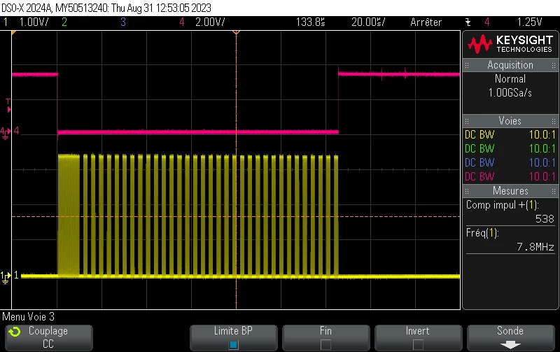
scope_105_full_run_clk.png

I'm surprised to see that the full read sequence is performed in burst of 7 bytes (14 clock cycles), spaced by approx 2µs delay between each burst. Since there is a FIFO on QSPI, there should no delay ? And why always 7 bytes bursts ?

While the transaction is running the CPU is running an infinite loop for debug.
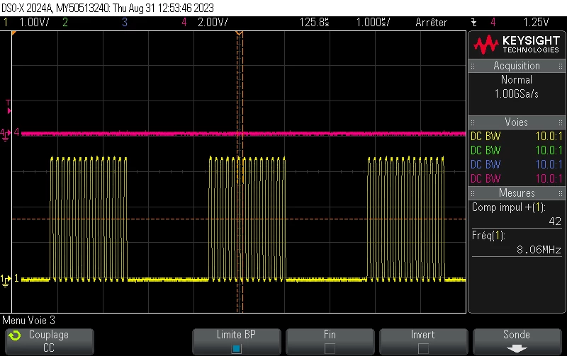
scope_107_burst_sequence.pngscope_106_burst_detail.png

That does not change if FifoThreshold is set to 1, 4 or 8. I have some difficulties to understand this parameter, in typical examples it is set to 4, but why ? Why 4 and not 1 ? What consequences on code ? Does it apply on DMA usage, or only for non DMA access (for "status register read" for example)

Another question : the datasheet suffers from absence of detailled chonograms about the "SampleShifting" parameter. Is it ok to let it at "NONE" ? (no circuitry added on the lines, short connection to the memory, and low frequency clock).

Here are the configurations :

QSPI and DMA modules config :

/* QUADSPI parameter configuration*/
hqspi.Instance = QUADSPI;
hqspi.Init.ClockPrescaler = 1;
hqspi.Init.FifoThreshold = 4;
hqspi.Init.SampleShifting = QSPI_SAMPLE_SHIFTING_NONE;
hqspi.Init.FlashSize = 25;
hqspi.Init.ChipSelectHighTime = QSPI_CS_HIGH_TIME_1_CYCLE;
hqspi.Init.ClockMode = QSPI_CLOCK_MODE_0;
hqspi.Init.FlashID = QSPI_FLASH_ID_1;
hqspi.Init.DualFlash = QSPI_DUALFLASH_DISABLE;

/* QUADSPI DMA Init */
/* QUADSPI Init */
hdma_quadspi.Instance = DMA2_Channel7;
hdma_quadspi.Init.Request = DMA_REQUEST_3;
hdma_quadspi.Init.Direction = DMA_PERIPH_TO_MEMORY;
hdma_quadspi.Init.PeriphInc = DMA_PINC_DISABLE;
hdma_quadspi.Init.MemInc = DMA_MINC_ENABLE;
hdma_quadspi.Init.PeriphDataAlignment = DMA_PDATAALIGN_BYTE;
hdma_quadspi.Init.MemDataAlignment = DMA_MDATAALIGN_BYTE;
hdma_quadspi.Init.Mode = DMA_NORMAL;
hdma_quadspi.Init.Priority = DMA_PRIORITY_MEDIUM;


QSPI read sequence :

uint8_t FLASH_Read_Page(uint32_t address, uint8_t * buffer, uint32_t lg)
{
// Configuring the command execution
qspi_flash_config.AddressSize = QSPI_ADDRESS_32_BITS;
qspi_flash_config.InstructionMode = QSPI_INSTRUCTION_1_LINE;
qspi_flash_config.DdrMode = QSPI_DDR_MODE_DISABLE;
qspi_flash_config.DdrHoldHalfCycle = QSPI_DDR_HHC_ANALOG_DELAY;
qspi_flash_config.SIOOMode = QSPI_SIOO_INST_EVERY_CMD;
qspi_flash_config.AlternateByteMode = QSPI_ALTERNATE_BYTES_NONE;
qspi_flash_config.AlternateBytes = 0;
qspi_flash_config.AlternateBytesSize = 0;

qspi_flash_config.Instruction = CMD_READ_4B_QUADIO_INOUT;
qspi_flash_config.AddressMode = QSPI_ADDRESS_4_LINES;
qspi_flash_config.Address = address;
qspi_flash_config.DummyCycles = 10;
qspi_flash_config.DataMode = QSPI_DATA_4_LINES;
qspi_flash_config.NbData = lg;

HAL_QSPI_Command(&hqspi_flash, &qspi_flash_config, 1000);

HAL_QSPI_Receive_DMA(&hqspi_flash, buffer);
}



This topic has been closed for replies.

6 replies

ST Technical Moderator
August 31, 2023

Hello @Aurelien Robert,

I guess you are using for the instruction command

CMD_READ_4B_QUADIO_INOUT

0xEC. If so, according to the datasheet, 1Line (instruction)+ 4Lines (address) + 2Lines (NbData lg)

FBelaid_0-1693491253585.png


1. Regarding FifoThreshold, it gives the number of valid bytes which are being held in the FIFO. 

In indirect mode, this bit is set when the FIFO threshold has been reached, or if there is any data left in the FIFO after reads from the Flash memory are complete. It is cleared automatically as soon as threshold condition is no longer true.
In automatic polling mode this bit is set every time the status register is read, and the bit is cleared when the data register is read.

2. Regarding sample shifting, SSHIFT bit allows the data to be sampled later in order to account for external signal delays. you may risk data corruption at high frequency if not enabled.

Hope this helps!

To give better visibility on the answered topics, please click on "Best answer" on the reply which solved your issue or answered your question.Best regards,FBL
Aurelien Robert
Associate III
August 31, 2023

I guess you are using for the instruction command

CMD_READ_4B_QUADIO_INOUT

0xEC. If so, according to the datasheet, 1Byte (instr)+ 4Bytes (address) + 2Bytes (NbData lg) which makes sense. 

FBelaid_0-1693491253585.png


Hello,

Yes, this is the command I used. Where do you see 2 bytes for the data ? I'm reading 256 bytes... My first screenshot show a total of 538 clock cycles : 8 (instruction) + 4*2 (address) + 10 (dummy) + 256*2 (data) = 538. The data transaction part of the screenshots is split into bursts of 7 bytes, and I still do not understand why, I don't see your point when you counting the instruction and the address here...

When doing the same thing for writing data, there are only bursts of 1 byte (2 clocks cycles), spaced by approx 200ns delay.


1. Regarding FifoThreshold, it gives the number of valid bytes which are being held in the FIFO. 

In indirect mode, this bit is set when the FIFO threshold has been reached, or if there is any data left in the FIFO after reads from the Flash memory are complete. It is cleared automatically as soon as threshold condition is no longer true.
In automatic polling mode this bit is set every time the status register is read, and the bit is cleared when the data register is read.


Okay, this is approximately what is written in the datasheet, but concretely, what values should I use for basic polling access (read status) or DMA access (read/write data) ? I'm using HAL functions (for the moment...). In my examples the value of 1 or 4 does not change anything, in which cases (applied to my situation) would I observe differences ?

2. Regarding sample shifting, SSHIFT bit allows the data to be sampled later in order to account for external signal delays. you may risk data corruption at high frequency if not enabled.


In SDR read mode, the memory puts the data on the falling edge of CLK, with a delay (<10ns for this memory), and the STM32 catches it at the rising edge (62ns later). In theory there would be no problem. If I enable sampling shifting, an extra half cycle is waited, so the line is read on the next falling edge of CLK, is that right ?

Thank you

Aurelien