
Solved
Unable to write Data into SPI2->DR register in stm32g030k6t6 MCU
Hello ,
I Have configured STM32G030K6t6 MCU has SPI master . I have used SPI2 Module. Chip select is controlled manually by GPIO .
I am unable to write exact data 0x79 in SPI2->DR register . Always it writes 0xff to DR and i am unable to read/Write anything from Slave. Kindly provide inputs
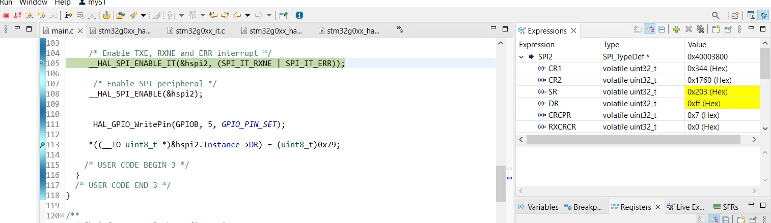
/**
 * @brief SPI2 Initialization Function
 * None
 * @retval None
 */
static void MX_SPI2_Init(void)
{

 /* USER CODE BEGIN SPI2_Init 0 */

 /* USER CODE END SPI2_Init 0 */

 /* USER CODE BEGIN SPI2_Init 1 */

 /* USER CODE END SPI2_Init 1 */
 /* SPI2 parameter configuration*/
 hspi2.Instance = SPI2;
 hspi2.Init.Mode = SPI_MODE_MASTER;
 hspi2.Init.Direction = SPI_DIRECTION_2LINES;
 hspi2.Init.DataSize = SPI_DATASIZE_8BIT;
 hspi2.Init.CLKPolarity = SPI_POLARITY_LOW;
 hspi2.Init.CLKPhase = SPI_PHASE_1EDGE;
 hspi2.Init.NSS = SPI_NSS_SOFT;
 hspi2.Init.BaudRatePrescaler = SPI_BAUDRATEPRESCALER_2;
 hspi2.Init.FirstBit = SPI_FIRSTBIT_MSB;
 hspi2.Init.TIMode = SPI_TIMODE_DISABLE;
 hspi2.Init.CRCCalculation = SPI_CRCCALCULATION_DISABLE;
 hspi2.Init.CRCPolynomial = 7;
 hspi2.Init.CRCLength = SPI_CRC_LENGTH_DATASIZE;
 hspi2.Init.NSSPMode = SPI_NSS_PULSE_DISABLE;
 if (HAL_SPI_Init(&hspi2) != HAL_OK)
 {
 Error_Handler();
 }
 /* USER CODE BEGIN SPI2_Init 2 */

 /* USER CODE END SPI2_Init 2 */

}

void HAL_SPI_MspInit(SPI_HandleTypeDef* hspi)
{
 GPIO_InitTypeDef GPIO_InitStruct = {0};
 if(hspi->Instance==SPI2)
 {
 /* USER CODE BEGIN SPI2_MspInit 0 */

 /* USER CODE END SPI2_MspInit 0 */
 /* Peripheral clock enable */
 __HAL_RCC_SPI2_CLK_ENABLE();

 __HAL_RCC_GPIOB_CLK_ENABLE();
 /**SPI2 GPIO Configuration
 PB6 ------> SPI2_MISO
 PB7 ------> SPI2_MOSI
 PB8 ------> SPI2_SCK
 */
 GPIO_InitStruct.Pin = GPIO_PIN_6;
 GPIO_InitStruct.Mode = GPIO_MODE_AF_PP;
 GPIO_InitStruct.Pull = GPIO_PULLUP;
 GPIO_InitStruct.Speed = GPIO_SPEED_FREQ_LOW;
 GPIO_InitStruct.Alternate = GPIO_AF4_SPI2;
 HAL_GPIO_Init(GPIOB, &GPIO_InitStruct);

 GPIO_InitStruct.Pin = GPIO_PIN_7|GPIO_PIN_8;
 GPIO_InitStruct.Mode = GPIO_MODE_AF_PP;
 GPIO_InitStruct.Pull = GPIO_NOPULL;
 GPIO_InitStruct.Speed = GPIO_SPEED_FREQ_LOW;
 GPIO_InitStruct.Alternate = GPIO_AF1_SPI2;
 HAL_GPIO_Init(GPIOB, &GPIO_InitStruct);

 /* SPI2 interrupt Init */
 HAL_NVIC_SetPriority(SPI2_IRQn, 0, 0);
 HAL_NVIC_EnableIRQ(SPI2_IRQn);
 /* USER CODE BEGIN SPI2_MspInit 1 */

 /* USER CODE END SPI2_MspInit 1 */
 }


/**
 * @brief This function handles SPI2 global interrupt.
 */
void SPI2_IRQHandler(void)
{
 /* USER CODE BEGIN SPI2_IRQn 0 */

 /* USER CODE END SPI2_IRQn 0 */
// HAL_SPI_IRQHandler(&hspi2);
	 FlagStatus tmp1;
	 FlagStatus tmp2;
	 FlagStatus tmp3;

	 tmp1 = __HAL_SPI_GET_FLAG(&hspi2, SPI_FLAG_RXNE)?SET:RESET;
	 tmp2 = __HAL_SPI_GET_IT_SOURCE(&hspi2, SPI_IT_RXNE);
	 tmp3 = __HAL_SPI_GET_FLAG(&hspi2, SPI_FLAG_OVR)?SET:RESET;
	 /* SPI in mode Receiver and Overrun not occurred ---------------------------*/
	 if ((tmp1 != RESET) && (tmp2 != RESET) && (tmp3 == RESET))
	 {
	 rx_isr();
	 }

 /* USER CODE BEGIN SPI2_IRQn 1 */

 /* USER CODE END SPI2_IRQn 1 */
}

* USER CODE BEGIN 1 */

/* USER CODE END 1 */
void rx_isr()
{
	uint8_t temp1;
	temp1 = *(__IO uint8_t *)&hspi2.Instance->DR;

	 HAL_GPIO_WritePin(GPIOB, 5, GPIO_PIN_RESET);

}