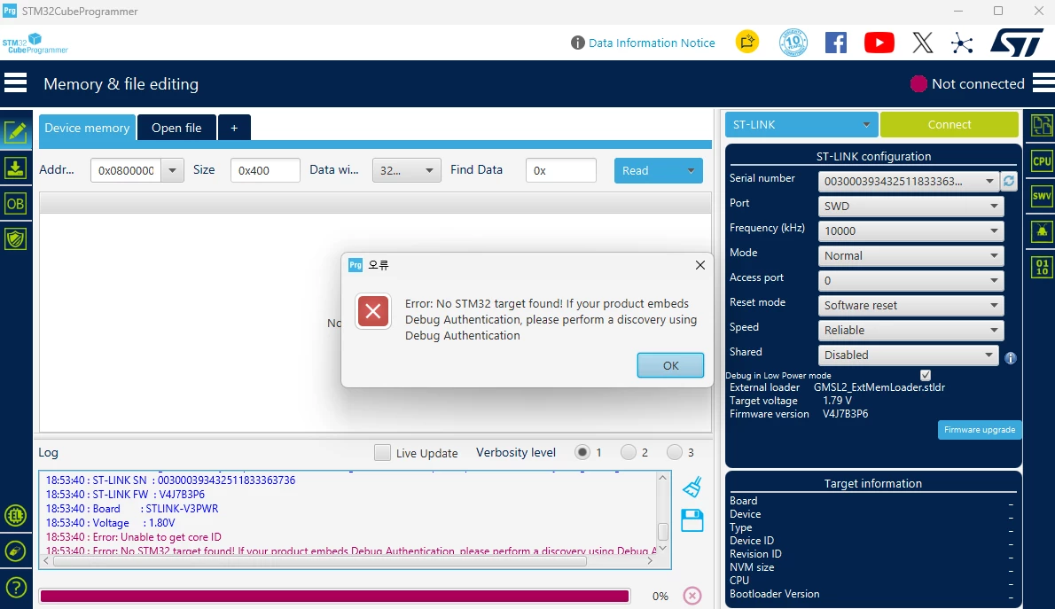
Unable to connect to STM32N657 after remapping BOOT1 from PA6 to PN10
Hello,
I am using an STM32N657 on a custom board.
I need to use PA6 as PIXCLK, so I would like to move the BOOT1 function from the default PA6 pin to PN10.
According to the STM32N6 BootROM/OTP description, I understood that BOOT1 can be remapped using OTP19 (BOOTROM_CONFIG_10):
I programmed OTP19 with 0x15200000 in STM32CubeProgrammer to change BOOT1 from PA6 to PN10.
Before programming OTP19, I could connect to the MCU normally through ST-LINK/SWD using PA6 as BOOT1.
However, after programming OTP19 to 0x15200000, I can no longer connect to the MCU.
The same issue has occurred on more than one custom board.
My test conditions are:
- MCU: STM32N657
- I/O supply voltage: 1.8 V
- BOOT1 remapped to: PN10
- OTP19 programmed value: 0x15200000
- PN10 is held HIGH before and during reset
- ST-LINK detects the target voltage
- During connection, STM32CubeProgrammer can sometimes identify Device ID 0x486, but then reports that the connection to device
0x486is lost - The board works and SWD connection is available before changing BOOT1 from PA6 to PN10
Could you please confirm the following?
- Is
OTP19 = 0x15200000the correct value for remapping BOOT1 to PN10 on STM32N657? - Are there any additional OTP settings required before using PN10 as BOOT1 when VDDIO3 is 1.8 V?
- Is there any known limitation or issue when using PN10 as the Development BOOT1 pin?
- After programming OTP19, is a specific power-cycle/reset sequence required for the new BOOT1 pin assignment to become effective?
- Is there any recovery method if the MCU can no longer enter Development Boot or connect through SWD after this OTP19 change?
I would appreciate it if you could also provide the recommended OTP configuration and programming sequence for changing BOOT1 from PA6 to PN10.
Best regards,