

Visitor II
Sep 18, 2026 10:14 AM UTC
Question

Unable to connect to STM32N657 after remapping BOOT1 from PA6 to PN10

Hello,

I am using an STM32N657 on a custom board.

I need to use PA6 as PIXCLK, so I would like to move the BOOT1 function from the default PA6 pin to PN10.

According to the STM32N6 BootROM/OTP description, I understood that BOOT1 can be remapped using OTP19 (BOOTROM_CONFIG_10):


I programmed OTP19 with 0x15200000 in STM32CubeProgrammer to change BOOT1 from PA6 to PN10.

Before programming OTP19, I could connect to the MCU normally through ST-LINK/SWD using PA6 as BOOT1.

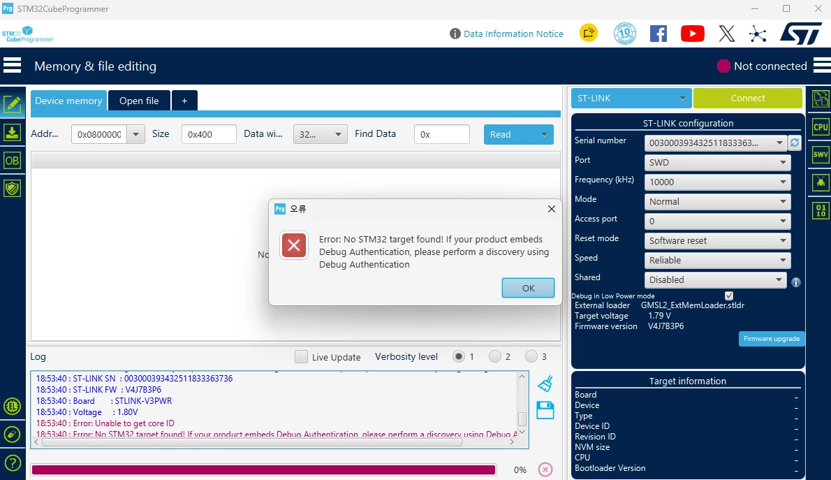
However, after programming OTP19 to 0x15200000, I can no longer connect to the MCU.

The same issue has occurred on more than one custom board.

My test conditions are:

  • MCU: STM32N657
  • I/O supply voltage: 1.8 V
  • BOOT1 remapped to: PN10
  • OTP19 programmed value: 0x15200000
  • PN10 is held HIGH before and during reset
  • ST-LINK detects the target voltage
  • During connection, STM32CubeProgrammer can sometimes identify Device ID 0x486, but then reports that the connection to device 0x486 is lost
  • The board works and SWD connection is available before changing BOOT1 from PA6 to PN10

Could you please confirm the following?

  1. Is OTP19 = 0x15200000 the correct value for remapping BOOT1 to PN10 on STM32N657?
  2. Are there any additional OTP settings required before using PN10 as BOOT1 when VDDIO3 is 1.8 V?
  3. Is there any known limitation or issue when using PN10 as the Development BOOT1 pin?
  4. After programming OTP19, is a specific power-cycle/reset sequence required for the new BOOT1 pin assignment to become effective?
  5. Is there any recovery method if the MCU can no longer enter Development Boot or connect through SWD after this OTP19 change?

I would appreciate it if you could also provide the recommended OTP configuration and programming sequence for changing BOOT1 from PA6 to PN10.

Best regards,


2 replies

mƎALLEm
ST Technical Moderator
Sep 21, 2026 9:36 AM UTC

Hello ​@CHACHA and welcome to the ST community,

The same question has been asked in this post:

The question has been already raised internally for review over the internal ticket CDM0065901 & CDM0065903  (not accessible by the community users).

To give better visibility on the answered topics, please click "Best answer" on the reply which solved your issue or answered your question.
mƎALLEm
ST Technical Moderator
Oct 26, 2026 12:49 PM UTC

Hello ​@CHACHA  and sorry for the late delay,

Our answer:

Here is a preliminary information while waiting for doc update.

UM3234/DS14791 and RM0486 (will be updated later) will be update with this content (approximate content for information only):

The BootROM is the first code executed after any system reset. The boot mode is determined by BOOT0 and BOOT1 pins, one OTP word (flash source selection), and one TAMP backup register.

• BOOT0 is a dedicated pin latched upon reset release

• BOOT1 is a non-dedicated boot pin. Its value can be sourced either from the default BOOT1 pin or from another GPIO from VDD power domain selected through the OTP system configuration (refer next table).

By default, PA6 is assigned as the BOOT1 input and is managed through the alternate function mechanism together with the SYSCFG_BOOTR register.

When another GPIO is selected as the BOOT1 source through the corresponding OTP configuration, the BOOT1 function on PA6 is masked and the input state of the selected GPIO is used instead and its pull-down default state remain enabled. 

Table1 BOOT1 available pins (package-specific pin availability not considered) 

PORTA

PORTB

PORTC

PORTD

PORTE

PORTF

PORTG

PORTH

PORTN

PORTO

PORTP

PORTQ

PA0

PB0

-

PD0

PE0

PF0

PG0

PH0

-

-

-

PQ0

PA1

PB1

-

PD1

PE1

PF1

PG1

PH1

-

-

-

PQ1

PA2

PB2

-

PD2

PE2

PF2

PG2

-

-

-

-

PQ2

PA3

PB3

-

PD3

PE3

PF3

PG3

PH3

-

-

-

PQ3

PA4

PB4

-

PD4

-

PF4

PG4

PH4

-

-

-

PQ4

PA5

PB5

-

PD5

PE5

PF5

PG5

PH5

-

-

-

PQ5

PA6(1)

PB6

-

PD6

PE6

PF6

PG6

PH6

-

-

-

PQ6

PA7

PB7

-

PD7

PE7

PF7

PG7

PH7

-

-

-

PQ7

PA8

PB8

-

PD8

PE8

PF8

PG8

PH8

-

-

-

-

PA9

PB9

-

PD9

PE9

PF9

PG9

-

-

-

-

-

PA10

PB10

-

PD10

PE10

PF10

PG10

-

-

-

-

-

PA11

PB11

-

PD11

PE11

PF11

PG11

-

-

-

-

-

PA12

PB12

-

PD12

PE12

PF12

PG12

-

-

-

-

-

PA13

PB13

PC13

PD13

PE13

PF13

PG13

-

-

-

-

-

PA14

PB14

PC14

PD14

PE14

PF14

PG14

-

-

-

-

-

PA15

PB15

PC15

PD15

PE15

PF15

PG15

-

-

-

-

-


(1) Default BOOT1 pin

Hope that answers your question.

To give better visibility on the answered topics, please click "Best answer" on the reply which solved your issue or answered your question.