

EngyCZ
Associate II
April 23, 2025
Question

Strange, unexpected behavior of memory bus pins during reset – silicon bug in STM32H743I rev. V

Hi.

  We found a serious problem in the behavior of the memory bus pins during reset.

Our design uses an STM32H743I CPU and non-volatile MRAM/FRAM memory connected via a bus. We use the FMC controller to access the memory, the bus pins are set up, and everything works. We have pull-up resistors on the nE[x] (chip select), nOE (output enable) and nWE (write enable) pins so that the correct levels are present on the memory inputs when the CPU starts. The problem occurs during a reset triggered, for example, by a watchdog or a reset button, when a negative glitch appears on these pins, causing an unwanted write to memory.

We have the same HW design equipped with STM32743I rev. Y (older than rev. V), where this problem is also manifested to a lesser extent and pull-up resistors compensate for it, but with rev. V the manifestation is significant.

The following are measurements on rev. Y and rev. V. We used the FMC_SRAM example from STM32Cube_FW_H7_V1.12.0, so we believe the FMC is initialized correctly.

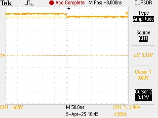
Our HW with STM32H743I rev. Y (Similar measurements were observed on the STM32H743I-EVAL board with rev. Y)

PD5 – nEW – glitch from 3.36V to 3.12V
EngyCZ_0-1745404604518.png


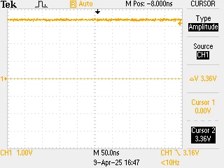
PD7 – FMC_nE1 – no glitch, stable 3.36V
EngyCZ_1-1745404604519.png


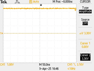
PG9 – FMC_nE2 – no glitch, stable 3.36V
EngyCZ_2-1745404604519.png


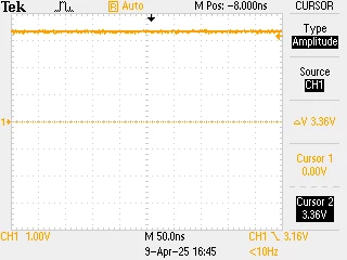
PG10 – FMC_nE3 – no glitch, stable 3.36V
EngyCZ_3-1745404604519.png


PG12 – FMC_nE4 – glitch from 3.36V to 2.48V
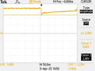
EngyCZ_4-1745404604519.png


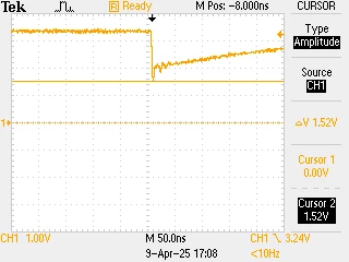
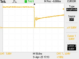
Our HW with STM32H743I rev. V

PD5 – nEW – glitch from 3.36V to 0V
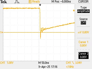
EngyCZ_5-1745404604519.png


PD7 – FMC_nE1 – glitch from 3.36V to 1.84V
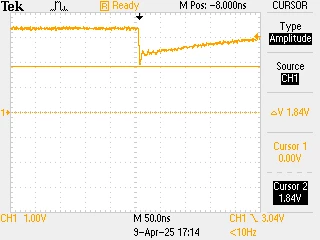
EngyCZ_6-1745404604520.png


PG9 – FMC_nE2 – glitch from 3.36V to 2.12V
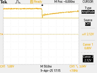
EngyCZ_7-1745404604520.png


PG10 – FMC_nE3 – glitch from 3.36V to 1.52V
EngyCZ_8-1745404604520.png


PG12 – FMC_nE4 – glitch from 3.36V to 0V
EngyCZ_9-1745404604521.png


From the documentation: “During and just after reset, the alternate functions are not active and most of the I/O ports are configured in analog mode“. So it looks like when the I/O pin is transitioning to the default state, the output is set to 0 for a while.

I would like to ask ST to investigate the problem, provide a SW workaround and mention the problem in the Errata document.

This topic has been closed for replies.

17 replies

Amel NASRI
ST Technical Moderator
April 30, 2025

Hi @EngyCZ ,

Interesting case where I don't have really a full explanation. But I would have a proposal to explore: is it possible for you to decrease the value of the external pull-up resistor on some pins where you noted the glitch? Does this have any impact?

-Amel

To give better visibility on the answered topics, please click on "Best Answer" on the reply which solved your issue or answered your question.
EngyCZ
EngyCZAuthor
Associate II
May 5, 2025

Hi @Amel NASRI 

Yes, we tried decreasing the value of the external pull-up resistor, but it had almost no effect on the glitch size. It only reduced the return time to 3.3V.

Bassett.David
Associate III
May 1, 2025

Hello EngyCZ,

I have no answer but wondering if writing these pins with "1" as GPIOs before enabling FMC control would make a difference?  Perhaps they "fall back" to the output register value as the FMC is disconnected during reset.  Hopefull I realize, but worth a try?

Regards,

Dave

EngyCZ
EngyCZAuthor
Associate II
May 5, 2025

Hi @Bassett.David 

Yes, we tried that too, but it had no effect.

Pavel A.
May 1, 2025

This chip has the nWE pin not for nothing. What if you link it to NRST so that write automatically gets disabled in unfortunate moments?


EngyCZ
EngyCZAuthor
Associate II
May 5, 2025

Hi @Pavel A. 

We measured the sequence of nWE and nRST pins and the nRST signal is activated much later, after the problems on the pins I described.

waclawek.jan
Super User
May 5, 2025

Hi @EngyCZ ,

> We measured the sequence of nWE and nRST pins and the nRST signal is activated much later, after the problems on the pins I described.

This is intriguing, as it defeats the very purpose of the nRST output signal (as a way to convey the internal reset signal to other circuitry). Here you are talking about the case when nRST occurs from "inside" the mcu, such as watchdog, I presume.

Would you have waveforms taken for this issue, can you please post them.

Also, what exactly is connected to nRST?

Sorry I have no comment relevant to your main issue.

Jan

EngyCZ
EngyCZAuthor
Associate II
May 5, 2025

Hi @waclawek.jan & @Pavel A. 

OK, a small correction. The voltage on the nRST pin starts to decrease simultaneously with the nWE glitch. However, it is not as fast as nWE probably because of the capacity 100nF on the input.

Thus, in the "digital" world, nRST switches to 0 later than nWE.


EngyCZ_0-1746443438404.png

nWE - Yellow, nRST - Blue

EngyCZ_1-1746443482589.png

EngyCZ_2-1746443496061.png

EngyCZ_3-1746443507146.png


Pavel A.
May 5, 2025

Which pin is nWE, PD5?  how it is configured (strength/speed, PU/PD) ? 

waclawek.jan
Super User
May 5, 2025

Thanks for the results with nRST. I now see that we are down at the nanoseconds realm.

If you are willing to experiment further, let's make a similar assumption then what @Bassett.David made above, i.e. that some portions of the whole circuitry reset faster than GPIO_MODER into Analog: let's assume that GPIO_AFR[] resets faster, disconnecting the pin driver from FMC itself (I presume that FMC wouldn't drive those pins to 0 under reset, an assumption which may be false, too). Now most of those pins don't have an explicit setting for GPIO_AFR[]=0, but I've seen cases where even if this was the case, some of the other signal sources was in fact connected.

So my experiment would be, to set given pins - while still being AF in GPIO_MODER - to GPIO_AFR[] = 0; and then try to experiment with the peripherals which are at the same pin, whether any of them would drive the output pin high. If it would, then I'd try to revert the pin to FMC while retaining that setting of that "other" peripheral, and invoke the reset.

I know it's a slim chance this would work; but let's be honest, what's the chance ST will provide a workaround here, or, more precisely, given the nature of the problem, what's the chance there *is* any sane workaround here.

JW

EngyCZ
EngyCZAuthor
Associate II
May 5, 2025

Thank @waclawek.jan for the suggestion.

On PD5 there is

AF2 - HRTIM_EEV3

AF7 - USART2_TX


HRTIM_EEV3 is the input signal for High resolution timer.

USART2_TX is Transmit Data Output for USART2, and according to the datasheet TX pin idle state is High.


I'm still waiting for the official ST statement @Amel NASRI.