

STM32N657: after programming OTP19 dev_boot_port/dev_boot_pin to relocate BOOT1 to PN10, device no longer enters development boot
Hello ST Team,
We have a custom STM32N657Z0H3Q board on which BOOT1 is routed to PN10 instead of the default PA6.
To configure the Boot ROM to sample BOOT1 from PN10, we programmed OTP Word 19 (BOOTROM_CONFIG_10) as described in RM0486 Rev. 4, Section 5, Table 18:
dev_boot_port [24:21] = 9→ Bank N (PN) →9 << 21 = 0x01200000dev_boot_pin [28:25] = 10→ Pin 10 →10 << 25 = 0x14000000- OTP19 =
0x15200000
Steps Followed
- Before programming, we read OTP through SWD. OTP19 was
0x00000000, with status0x00000000, indicating that it was unprogrammed and not write-locked. SWD/ST-LINK access was working normally. - We programmed OTP19 with
0x15200000using STM32CubeProgrammer v2.23.0, without enabling the lock option. The tool reported:- "OTP words programming done successfully"
-
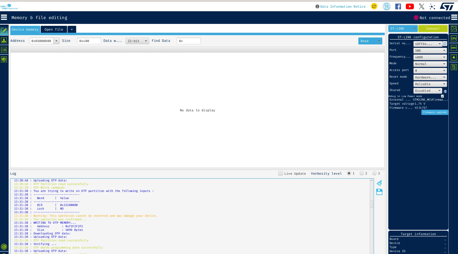
- After the next power cycle/reboot, the device no longer enters Development Boot. Instead, it boots from Flash, and our FSBL and application start running normally. SWD/debug access is no longer available.
Same Issue Already Reported
After encountering this issue, we found an existing ST Community topic describing what appears to be the same problem on a different custom board:
ST Community – Unable to connect to STM32N657 after remapping BOOT1 from PA6 to PN10
The reported case involves the same MCU, the same PA6 → PN10 remapping, the same OTP19 value 0x15200000, and the same loss of SWD access after programming OTP19.
Questions
Q1. Is OTP19 = 0x15200000 the correct value for selecting PN10 as the BOOT1 source?
Specifically, are the following field values correct?
dev_boot_port = 9→ Bank N (PN)dev_boot_pin = 10→ PN10
Q2. Is any specific power-cycle or reset sequence required after programming OTP19 for the new BOOT1 pin assignment to take effect?
Q3. Is there any recovery procedure to regain debug access on a device where OTP19 has already been programmed to select a BOOT1 pin that cannot be sampled high?
We understand that OTP bits cannot be cleared once programmed.
Request for Confirmation
We have already lost one board due to this issue, so we would like to avoid risking another board without a confirmed procedure.
Could you please verify this configuration on your side and confirm:
- Whether PN10 can be used as BOOT1 on the STM32N657Z0H3Q package.
- Whether
OTP19 = 0x15200000is the correct configuration. - The exact programming and power-cycle/reset sequence that should be followed.
- Whether there is any recovery method for the board that has already been programmed.
- If PN10 is not usable as BOOT1 on this package, please confirm this so that we can avoid programming the same configuration on another board.
A confirmed working procedure, or confirmation that PN10 cannot be used as BOOT1 on this package, would help us proceed with the board bring-up safely.
Since the same issue has already been reported in the ST Community and remains unresolved, we would greatly appreciate your prompt assistance.
Best regards,
Richu