STM32N6 FMC SDRAM: what does "Primary interfaces used" mean, and which pins are the primary ones?
Hello,
We are designing a board with STM32N647X0H3Q (VFBGA264) and a 16-bit SDR SDRAM
(512 Mbit, x16, 3.3 V LVTTL) on the FMC, and we would like to run SDCLK at 133 MHz
and 166 MHz.
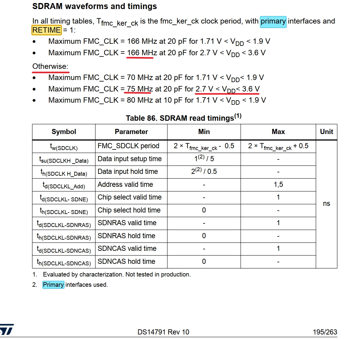
In DS14791 Rev 10, section "SDRAM waveforms and timings", the text says:
"In all timing tables, Tfmc_ker_ck is the fmc_ker_ck clock period, with primary
interfaces and RETIME = 1:
- Maximum FMC_CLK = 166 MHz at 20 pF for 2.7 V < VDD < 3.6 V
Otherwise:
- Maximum FMC_CLK = 75 MHz at 20 pF for 2.7 V < VDD < 3.6 V"
and Tables 86 to 89 have note 2: "Primary interfaces used."
However, I could not find a definition of "primary interfaces" anywhere in DS14791,
RM0486, AN5967 or ES0620, and the CubeMX device database shows no difference between
the alternative pins of the same FMC signal.
On VFBGA264, the control, address, SDCLK and NBL signals each have only one pin, but
every data line has two or three possible pins (all AF12), for example:
Signal Option 1 Option 2 Option 3
FMC_D0 PB15 PA12 -
FMC_D1 PB8 PA11 -
FMC_D2 PB2 PA10 -
FMC_D3 PB9 PA9 -
FMC_D4 PD13 PA8 -
FMC_D5 PB13 PA2 -
FMC_D6 PD5 PA1 -
FMC_D7 PB14 PA0 -
FMC_D8 PD11 PG9 PC3
FMC_D9 PE0 PB12 -
FMC_D10 PE1 PB11 -
FMC_D11 PE2 PB10 -
FMC_D12 PE3 PB5 -
FMC_D13 PB0 PB4 -
FMC_D14 PB6 PC0 -
FMC_D15 PB7 PA15 -
My questions:
1. What exactly does "primary interfaces" mean for the FMC SDRAM timings?
2. Which pin for each of FMC_D0 to FMC_D15 belongs to the primary interface on
VFBGA264? Are the control/address/SDCLK/NBL pins (single option) all primary?
3. We may also use VFBGA178 (STM32N645I0H3Q). On that package some data lines have
only one option (for example FMC_D0 = PA12 only). Which pins are primary on
VFBGA178, and is 166 MHz possible there at all?
Thank you in advance.