

STM32H743VG - gap in FLASH bank adresses
Hi,
Context:
I've hit a roadblock in using the stm32h743VG.
According the reference manual, this is the FLASH memory mapping:
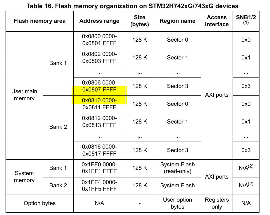
I'd like to focus your attention on the address gap between Bank1 & Bank2.
To alleviate this, I've first done the following:
MEMORY
 {
- FLASH (rx) : ORIGIN = 0x08000000, LENGTH = 1024K
+ FLASH_1 (rx) : ORIGIN = 0x08000000, LENGTH = 512K
+ FLASH_2 (rx) : ORIGIN = 0x08100000, LENGTH = 512K
This prevents corruption, as the linker initially tried to store functions in the address gap.
But this is cumbersome, as I need to use more than 512K for my `.text` output section.
Question:
Is there a way to define the FLASH region like this:
(EDIT: fixed 128k to 512k)
MEMORY
{
 FLASH (rx) : ORIGIN = 0x08000000, LENGTH = 1024K + 512K
/* Add 512K, which is the size of the gap between banks */
And prevent the linker to use the addresses between 0x08080000 and 0x0809FFFF ?
Alternative question:
Is there a syntax that would allow me to take all `*(.text)` and `*(.text*)` input sections up until they don't fit in FLASH_1, fit that into an output section named `.text_1`, then taking the remaining `*(.text*)` input sections and fit them into `.text_2` which would go into `FLASH_2` ?
