Associate III
October 3, 2026
Solved

STM32G474 square wave present on OSC_OUT when in bypass mode

  • October 3, 2026
  • 5 replies
  • 38 views

We have a G474 with a 12 MHz oscillator feeding into PF0/OSC_IN and have the device configured in bypass mode. We’re trying to use PF1/OSC_OUT as an ADC input, however we’re seeing a 300mV peak-peak square wave on the pin when our 2 kohm signal is connected to it.

Our layout really doesn’t leave enough room for this to be crosstalk, especially since we’re seeing a clean square wave. Is there something internally that could be leaving some clock circuitry connected?

For our purposes we can work around the extra noise in software; however, if we do we’d like to ensure that we won’t have any long-term reliability issues from feeding a signal into the clock circuitry.
Best answer by AScha.3

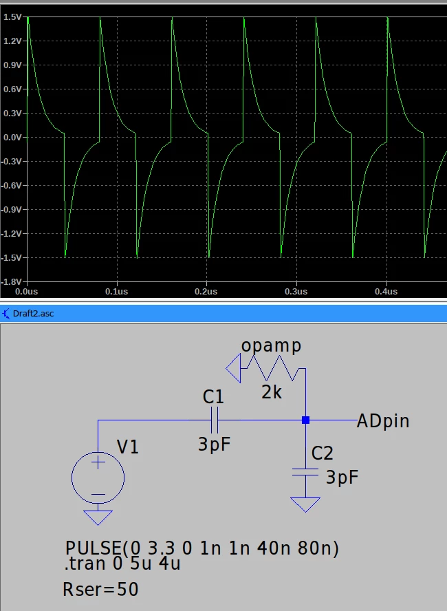
Such things difficult to measure...so check a simple simu first, what could happen :

coupling the 12MHz 3vss ---- 3pF  stray cap. ----to 2 k impedance :

(3pF = about 1p stray + about 2p inside the case metal to epoxy mold)


+

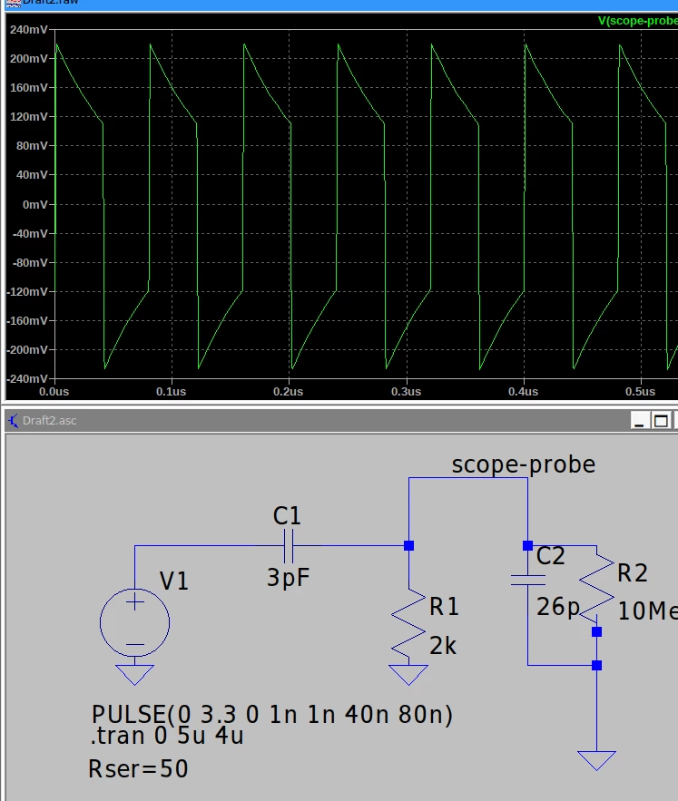
now with the scope probe at the pin: (26 pF )


+

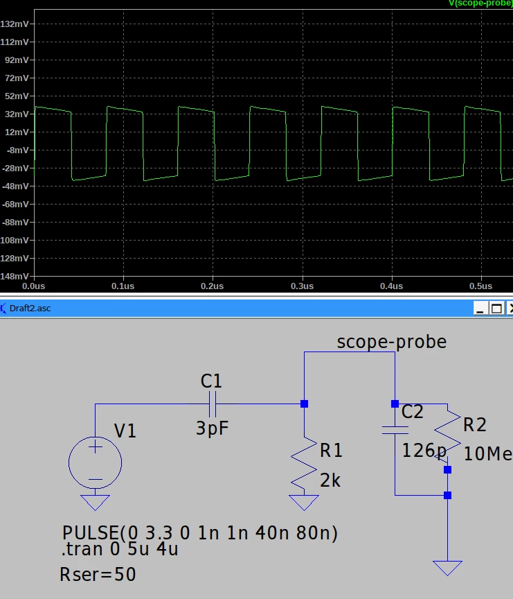
now with 120pF  probe (almost a 1:1 setting at the probe)


This looks almost same as your measurement. So you know… its just, what is to be expected, on a pin to pin , 12Mhz to analog IN .

So its just physics, nothing about the cpu involved or the opamp.

If you want it “better”, you have to change the circuit (= physical effects): reduce coupling - >  use more distant pin clock to analog IN; or give the analog in higher capacity , to reduce the coupling; if needed bandwidth on pin allows, put a cap direct at the pin to gnd.

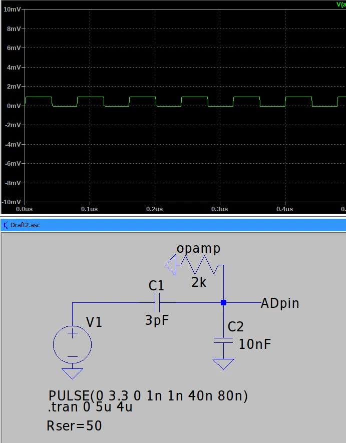
so with 10nF at the pin:

Now 0.9 mVss crosstalk.

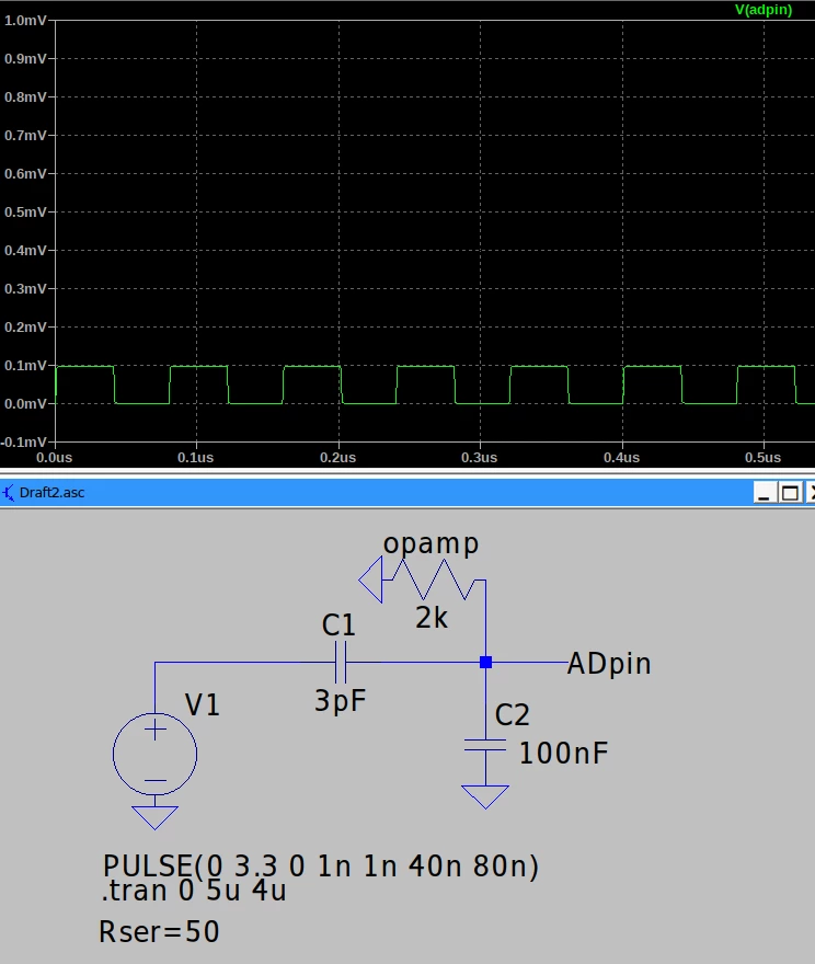
  + with 100nF (+2k from opamp giving about 1kHz analog signal bandwidth)

now 100 uVpp !

5 replies

liampwllAuthor
Associate III
October 3, 2026

Here’s the layout and waveform for reference. The only path for coupling outside of the IC is at the pins themselves and it looks too square to be capacitive coupling given that the input is driven from an op-amp with a 2 kohm resistor on it and absolutely no capacitors. I also put a shorter ground on the probe and it’s only 160 mV p-p.


AScha.3
AScha.3Best answer
Super User
October 3, 2026

Such things difficult to measure...so check a simple simu first, what could happen :

coupling the 12MHz 3vss ---- 3pF  stray cap. ----to 2 k impedance :

(3pF = about 1p stray + about 2p inside the case metal to epoxy mold)


+

now with the scope probe at the pin: (26 pF )


+

now with 120pF  probe (almost a 1:1 setting at the probe)


This looks almost same as your measurement. So you know… its just, what is to be expected, on a pin to pin , 12Mhz to analog IN .

So its just physics, nothing about the cpu involved or the opamp.

If you want it “better”, you have to change the circuit (= physical effects): reduce coupling - >  use more distant pin clock to analog IN; or give the analog in higher capacity , to reduce the coupling; if needed bandwidth on pin allows, put a cap direct at the pin to gnd.

so with 10nF at the pin:

Now 0.9 mVss crosstalk.

  + with 100nF (+2k from opamp giving about 1kHz analog signal bandwidth)

now 100 uVpp !

If you feel a post has answered your question, please click on " Best Answer ".
liampwllAuthor
Associate III
October 3, 2026

I did not consider the probe, although it was in 10x and it really doesn’t look like there’s enough decay happening. I can probably shuffle things around to put the input on another pin, although we only noticed it because we were seeing a large offset which is fixed by just changing the sample time.

Associate II
October 3, 2026

​@liampwll 

PF0 and PF1 are a pair of pins often used with an external Crystal oscillator.  It should be possible to leave PF0 as RCC_OSC_IN and reconfigure PF1 as an alternate for ADC2_IN10 analogue input.

Its possible your reconfiguration is not fully detaching PF1 . Here are what the start up configuration has to do:-

  • enable GPIOF Clock in AHB2ENR          // turn GPIO clock on for port F
  • select PF1 as alternate AF0 in GPIOF+AFRL  //select alternate for PF1 as  ADC2_IN10
  • select PF1 as analogue input in GPIOF+MODER  //select PF1 as an analogue input.

You could also use the internal HSI RC oscillator, abandon feeding 12MHz into PF0 and configure PF0 as input/analogue input.

If that does not solve your problem the other possibility is some kind of residue under the MCU shorting pins, you could check resistance between PF0 and PF1 with power off.

MM..1
Super User
October 3, 2026

Seems as normal analog crosstalk , bad pcb routing result. 100mV amplitude on your scoped is maybe missed reference gnd layer etc. Too choice pins ADC ahead any clock is bad idea.