STM32G431: ADC1 channel sequence confusion
Heyho,
I’m confused - or the STM32G431KBU (in QFN32) is…
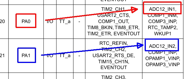
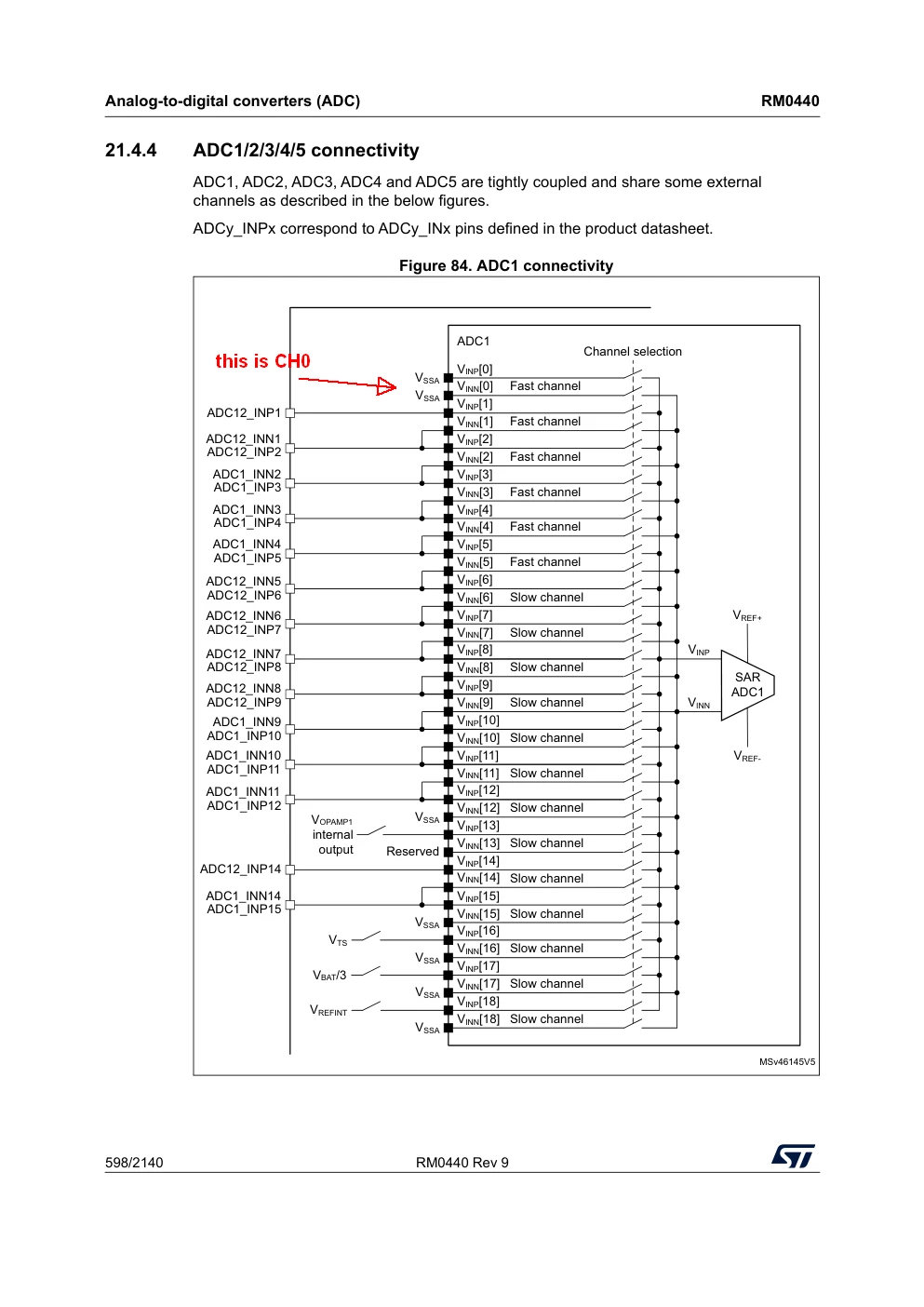
I’m using ADC 1 with 2 external inputs, PA0, PA1, and the internal “REFI” and temperature channel “TEMP”.
All running with continuous and circular DMA in the background, no interrupts. If I need an ADC value, I simply grab it from the ADC DMA buffer.
This is basically working, except for the channel sequence. Which I set manually, but have at least triple-checked the SQR1 / SQR2 values with the RM...
If I set up the channel sequence in ADC1->SQR1 in the order: PA0, PA1, REFI, TEMP, then I find in the DMA buffer instead of this order: 0, PA0, REFI, TEMP
→ so PA0 was “shifted”, PA1 is nowhere to be found (it is not 0, checked the GPIO via scope).
If I add and insert a dummy channel “VDMY” as the first in the sequence, so that the sequence should result in VDMY, PA0, PA1, REFI, TEMP, I find this order in the DMA buffer:
PA1, VDMY, PA0, REFI, TEMP
At least I get all the channels now, the measurement data is correct.
So, what am I messing up in the ADC & DMA setup?
Something in the init sequence concerning DMA / ADC ?
u16Adc1DmaBuf[80]

00 1313 0000 1972 1504 0936
05 1313 0000 1972 1504 0936
10 1313 0000 1972 1504 0936
15 1313 0000 1972 1504 0936
20 1313 0000 1972 1503 0936
25 1313 0000 1972 1504 0936
30 1313 0000 1972 1504 0936
35 1313 0000 1972 1504 0936
40 1313 0000 1972 1503 0936
45 1313 0000 1972 1504 0936
50 1313 0000 1972 1504 0936
55 1313 0000 1972 1504 0936
60 1313 0000 1972 1504 0936
65 1313 0000 1972 1504 0936
70 1313 0000 1972 1504 0936
75 1313 0000 1972 1504 0936
*** end
   VDMY PA0  PA1  REFI TEMP <- that' what it should be, but it is:
   PA1  VDMY PA0  REFI TEMP
The ADC registers:
ADC1->
ISR   0000000B
IER   00000000
CR    10000005
CFGR  80003003
CFGR2 000000D5
SMPR1 36DB6DB6
SMPR2 06DB6DB6
SQR1  12040084
SQR2  00000010
SQR3  00000000
SQR4  00000000
DR    00000000
CALFACT 0000003A
OFR1   00000000
OFR2   00000000
OFR3   00000000
OFR4   00000000
DIFSEL 00000000

ADC12_COMMON->
CSR 0000000B
CCR 00D00000
CDR 00000000

DMA1_Channel3->
CCR   000015A9
CNDTR 27
CMAR      20000A24
CPAR      50000040
&ADC1->DR 50000040
And here’s the ADC & DMA init and start:
/* +++++++++++++++++++++++++++++++++++++++++++++++++++++++++++++++++++++++ */
/* ADC1 init function
 */
uint8_t Adc1Init(void)
{
	uint32_t u32StartTick = 0;

	/* ++++++++++++++++++++++++++++++++++++++++++++++++++++ */
	/* ADC1 clock enable */
	if( (RCC->AHB2ENR & RCC_AHB2ENR_ADC12EN) != RCC_AHB2ENR_ADC12EN )
	{
		__IO uint32_t u32TmpReg;

		RCC->AHB2ENR |= RCC_AHB2ENR_ADC12EN;
		u32TmpReg = ( RCC->AHB2ENR & RCC_AHB2ENR_ADC12EN );
		(void)u32TmpReg;
	}

	/* ++++++++++++++++++++++++++++++++++++++++++++++++++++ */
	/* register reset */
	ADC1->CR 		= 0;
	ADC1->CFGR 		= 0;
	ADC1->CFGR2 	= 0;
	ADC1->SMPR1 	= 0;
	ADC1->SMPR2 	= 0;

	/* sequence set later */
	ADC1->SQR1 		= 0;
	ADC1->SQR2 		= 0;
	ADC1->SQR3 		= 0;
	ADC1->SQR4 		= 0;

	/* no offsets */
	ADC1->OFR1		= 0;
	ADC1->OFR2		= 0;
	ADC1->OFR3		= 0;
	ADC1->OFR4		= 0;
	/* single-ended */
	ADC1->DIFSEL 	= 0;

	/* no interrupts */
	ADC1->IER 	= 0;
	ADC1->ISR 	= 0x000007FF;

	ADC12_COMMON->CCR = 0;

	/* ++++++++++++++++++++++++++++++++++++++++++++++++++++ */
	/* GPIO & DMA init */
	Adc1GpioDmaInit();

	/* ++++++++++++++++++++++++++++++++++++++++++++++++++++ */
	/* register settings */

	/* CFGR
	 *	JQ disable,
	 *	continuous & overrun mode,
	 *	DMA set later: DMA circular, DMA on
	 */
	ADC1->CFGR 	= ( ADC_CFGR_JQDIS |
					ADC_CFGR_CONT | ADC_CFGR_OVRMOD );

	/* CFGR2
	 *	oversampling:
	 *		enable, x64, shift 6
	 */
	ADC1->CFGR2 = ( ADC_CFGR2_ROVSE |
					(ADC_CFGR2_OVSR_2 | ADC_CFGR2_OVSR_0) |
					(ADC_CFGR2_OVSS_2 | ADC_CFGR2_OVSS_1) );

	/* ++++++++++++++++++++++++++++++++++++++++++++ */
	/* sampling CYCLE time, same for all channels */
#if( 0 )
	ADC1->SMPR1 = 0x00000036;
	ADC1->SMPR2 = 0x06180000;
#elif( 1 )
	ADC1->SMPR1 = 	(	(ADC_SAMPLTIME_CYCLES_ALL <<  0) | (ADC_SAMPLTIME_CYCLES_ALL <<  3) | (ADC_SAMPLTIME_CYCLES_ALL <<  6) |
						(ADC_SAMPLTIME_CYCLES_ALL <<  9) | (ADC_SAMPLTIME_CYCLES_ALL << 12) | (ADC_SAMPLTIME_CYCLES_ALL << 15) |
						(ADC_SAMPLTIME_CYCLES_ALL << 18) | (ADC_SAMPLTIME_CYCLES_ALL << 21) | (ADC_SAMPLTIME_CYCLES_ALL << 24) |
						(ADC_SAMPLTIME_CYCLES_ALL << 27) );
	ADC1->SMPR2 = 	(	(ADC_SAMPLTIME_CYCLES_ALL <<  0) | (ADC_SAMPLTIME_CYCLES_ALL <<  3) | (ADC_SAMPLTIME_CYCLES_ALL <<  6) |
						(ADC_SAMPLTIME_CYCLES_ALL <<  9) | (ADC_SAMPLTIME_CYCLES_ALL << 12) | (ADC_SAMPLTIME_CYCLES_ALL << 15) |
						(ADC_SAMPLTIME_CYCLES_ALL << 18) | (ADC_SAMPLTIME_CYCLES_ALL << 21) | (ADC_SAMPLTIME_CYCLES_ALL << 24) );
#else
	ADC1->SMPR1 = 	(	(ADC_SAMPLTIME_CYCLES_ALL <<  0) | (ADC_SAMPLTIME_CYCLES_ALL <<  3) );
	ADC1->SMPR2 = 	(	(ADC_SAMPLTIME_CYCLES_ALL << 18) | (ADC_SAMPLTIME_CYCLES_ALL << 24) );
#endif

	/* ++++++++++++++++++++++++++++++++++++++++++++ */
	/* channel SEQUENCER configuration */
#if( 0 )
	ADC1->SQR1 = 0x10481003;
#else
	ADC1->SQR1 = 0;
	ADC1->SQR2 = 0;
	Adc1ConfigChannelSeq(ADC_CHANNEL_EXT_2,  1);
	Adc1ConfigChannelSeq(ADC_CHANNEL_EXT_0,  2);
	Adc1ConfigChannelSeq(ADC_CHANNEL_EXT_1,  3);
	Adc1ConfigChannelSeq(ADC_CHANNEL_INT_18, 4);
	Adc1ConfigChannelSeq(ADC_CHANNEL_INT_16, 5);
	/* sequence length */
	ADC1->SQR1 |= (uint32_t)(ADC_CHANNELS_NUM - 1);
#endif

	/* ++++++++++++++++++++++++++++++++++++++++++++ */
	/* wake up temperature sensor / enable "internal path" to ADC */
	ADC12_COMMON->CCR |= ADC_CCR_VSENSESEL;
	/* enable VREFINT "internal path" to ADC */
	ADC12_COMMON->CCR |= ADC_CCR_VREFEN;
	/* set prescaler */
	ADC12_COMMON->CCR |= ADC_CCR_PRESC_2;

	/* ++++++++++++++++++++++++++++++++++++++++++++ */
	/* voltage regulator enable */
	ADC1->CR |= ADC_CR_ADVREGEN;
	u32StartTick = HAL_GetTick();
	while( (HAL_GetTick() - u32StartTick) < (uint32_t)ADC_TIMEOUT_MS_REGEN );

	/* ++++++++++++++++++++++++++++++++++++++++++++ */
	/* calibration */
	ADC1->CR &= ~ADC_CR_ADEN;
	ADC1->CR |= ADC_CR_ADCAL;
	u32StartTick = HAL_GetTick();
	while( 	((HAL_GetTick() - u32StartTick) < (uint32_t)ADC_TIMEOUT_MS_CAL) &&
			((ADC1->CR & ADC_CR_ADCAL) == ADC_CR_ADCAL) );

	if( (ADC1->CR & ADC_CR_ADCAL) == ADC_CR_ADCAL )
	{
		#if DEBUG_ADC_ERR
			uart_printf(SZC_TEXT_ERR "ADC CAL\n\r");
			uart_printf("CR %08lX\n\r", ADC1->CR);
			uart_printf(SZC_TEXT_ERR "ADC not started\n\r");
		#endif	/* DEBUG_ADC_ERR */

		return HAL_ERROR;
	}

	/* ++++++++++++++++++++++++++++++++++++++++++++ */
	/* DMA start */
	Adc1DmaStart();

	/* ADC enable */
	ADC1->CR |= ADC_CR_ADEN;

	/* wait for ADC RDY */
	u32StartTick = HAL_GetTick();
	while( 	((HAL_GetTick() - u32StartTick) < (uint32_t)ADC_TIMEOUT_MS_RDY) &&
			((ADC1->ISR & ADC_ISR_ADRDY) == 0) );

	if( (ADC1->ISR & ADC_ISR_ADRDY) == 0 )
	{
		#if DEBUG_ADC_ERR
			uart_printf(SZC_TEXT_ERR "ADC ADRDY\n\r");
			uart_printf("ISR %08lX\n\r", ADC1->ISR);
			uart_printf(SZC_TEXT_ERR "ADC not started\n\r");
		#endif	/* DEBUG_ADC_ERR */

		return HAL_ERROR;
	}

	/* ++++++++++++++++++++++++++++++++++++++++++++ */
	/* start ADC */
	ADC1->CR |= ADC_CR_ADSTART;

	return HAL_OK;
}


/* +++++++++++++++++++++++++++++++++++++++++++++++++++++++++++++++++++++++ */
/* ADC1
 *	clock, GPIO & DMA init
 */
void Adc1GpioDmaInit(void)
{
	/* ++++++++++++++++++++++++++++++++++++++++++++++++++++ */
	/* ADC1 GPIO Configuration
	 *		PA0	------> "ADM_IN0" in schematic
	 *			-> VPWR = ~ 5V, divider 47k / 22k
	 *		PA1	------> "ADM_IN1" in schematic
	 *			-> VRECT = ~ 6V..12V, divider 47k / 10k
	 */
	GPIO_InitTypeDef GPIO_InitStruct = { 0 };

	/* clock enabled in gpio.c */

	GPIO_InitStruct.Pin 	= ADC_IN0_Pin | ADC_IN1_Pin;
	GPIO_InitStruct.Mode 	= GPIO_MODE_ANALOG;
	GPIO_InitStruct.Pull 	= GPIO_NOPULL;
	HAL_GPIO_Init(ADC_IN_GPIO_Port, &GPIO_InitStruct);

	/* ++++++++++++++++++++++++++++++++++++++++++++++++++++ */
	/* DMA init */
	DMA1_Channel3->CCR 		= 0;
	DMA1_Channel3->CPAR 	= (uint32_t)&ADC1->DR;
	DMA1_Channel3->CMAR 	= (uint32_t)u16Adc1DmaBuf;
	DMA1_Channel3->CNDTR 	= 0;	/* later = (uint32_t)ADC_DMA_BUF_SIZE; */

	/* DMA MUX
	 *	ATTENTION: MUX channel = DMA channel - 1
	 */
	DMAMUX1_Channel2->CCR = DMA_REQUEST_ADC1;

	/* clear DMA flags */
	DMA1->IFCR = DMA_IFCR_CGIF3;

	/* CCR */
	DMA1_Channel3->CCR 	= ( DMA_CCR_PL_0 |
							DMA_CCR_MSIZE_0 | DMA_CCR_PSIZE_0 |
							DMA_CCR_MINC |
							DMA_CCR_CIRC |
							DMA_CCR_TEIE );
}


/* +++++++++++++++++++++++++++++++++++++++++++++++++++++++++++++++++++++++ */
/* ADC1 channel sequence setting
 *	channel & rank
 */
uint8_t Adc1ConfigChannelSeq(uint32_t u32Channel, uint32_t u32Rank)
{
	if( (ADC1->CR & ADC_CR_ADSTART) != 0 ) return HAL_BUSY;

	/* set bit shift */
	uint32_t u32Shift = (uint32_t)(u32Rank * ADC_RANK_BASE_1);
	/* set SQRx register */
	volatile uint32_t *pu32Reg = &ADC1->SQR1;

	/* check rank */
	if( u32Rank > 4 )
	{
		pu32Reg = &ADC1->SQR2;
		u32Rank -= 4;
		u32Shift = (uint32_t)((u32Rank - 1) * ADC_RANK_BASE_1);
	}

	pu32Reg += (uint32_t)(((u32Shift & ADC_REG_SQRX_REGOFFSET) >> ADC_SQRX_REGOFFSET_Pos) << 2UL);

	/* clear rank */
	*pu32Reg &= ~(ADC_RANK_CHNL_MASK << (u32Shift & ADC_RANK_CHNL_MASK));
	/* set channel to rank */
	*pu32Reg |= (u32Channel << (u32Shift & ADC_RANK_CHNL_MASK));

	return HAL_OK;
}


/* +++++++++++++++++++++++++++++++++++++++++++++++++++++++++++++++++++++++ */
/* ADC DMA start or re-start
 */
void Adc1DmaStart(void)
{
	/* stop if still running */
	if( u8Adc1DmaActive != 0 ) Adc1DmaStop();

	DMA1_Channel3->CCR &= ~DMA_CCR_EN;

	/* clear DMA flags */
	DMA1->IFCR = DMA_IFCR_CGIF3;

	DMA1_Channel3->CPAR 	= (uint32_t)&ADC1->DR;
	DMA1_Channel3->CMAR 	= (uint32_t)u16Adc1DmaBuf;
	DMA1_Channel3->CNDTR 	= (uint32_t)ADC_DMA_BUF_SIZE;

	/* clear ADC (DMA) flags ? */
	ADC1->ISR = (uint32_t)0x7FE;

	/* DMA enable */
	DMA1_Channel3->CCR |= DMA_CCR_EN;

	/* peripheral DMA enable */
	ADC1->CFGR 	|= ADC_CFGR_DMACFG;
	ADC1->CFGR 	|= ADC_CFGR_DMAEN;

	u8Adc1DmaActive = 1;
}
Thanks in advance!