sean lannon
Associate II
July 10, 2017
Solved

STM32F411CC - (256kB) Flash Sectors

  • July 10, 2017
  • 8 replies
  • 3395 views
Posted on July 10, 2017 at 18:49

Can anyone confirm what the Flash sector sizes are on this MCU version?

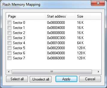
All documentation lumps the F411xC with the F411xE even though the former has 256kB of flash, and the latter has 512kB. The stm32f4xx_hal_flash_ex header defines the same number of sectors as the F411xE, so I'm assuming all the sectors for the STM32F411CC are just half of all the sectors outlined in the datasheet (RM0383 / DocID026448 Rev 1 - page 43).

The ST-LINK tool > Erase sectors option matches the datasheet, which is misleading as it shows a total of 512kB when counting up each sector!

0690X00000607UiQAI.png

I just want to be 100% certain. My guess is that the sectors are using the same Start address but have the following sizes:

  • Sector 0: 8K
  • Sector 1: 8K
  • Sector 2: 8K
  • Sector 3: 8K
  • Sector 4: 32K
  • Sector 5: 64K
  • Sector 6: 64K
  • Sector 7: 64K

Thanks!

#stm32f4xx-flash #flash-stm32 #stm32f411cc

This topic has been closed for replies.
Best answer by Tesla DeLorean
Posted on July 11, 2017 at 13:00

Yeah, sorry should have been 16-bit, typing quickly from memory.

>>t

hat there is 256kB of flash on the die

More like there is 512KB on all the die, and in your case they only spent time testing 256KB of it.

>>

Or there are the same number of sectors at half capacity..

Really not how this works.

Used to buy F205 parts with 256KB for a product, they all had 1MB on-die. 

Time on the tester is very expensive, the tester is expensive so they'll only have a few, Flash is very slow to erase and write multiple times, the flash test is going to take longer than most other logic on the rest of the IC, so they increase throughput by testing a fraction of the memory on some devices and create price stratification. They use one die because you have less work to do characterizing/validating the design, and less packaging/fixturing, and less reconfiguration between runs of wafer/die.

A data sheet covering multiple memory and pin devices is typically describing a single die whose performance they have characterized, and meets (defines) the published specs.

8 replies

Tesla DeLorean
Guru
July 11, 2017
Posted on July 11, 2017 at 02:28

Pretty sure it's not that, the two parts likely share a common die.

16 + 16 + 16 + 16 + 64 + 128 = 256

Tips, Buy me a coffee, or three.. PayPal Venmo (See Profile) Up vote any posts that you find helpful, it shows what's working..
Tesla DeLorean
Guru
July 11, 2017
Posted on July 11, 2017 at 02:40

printf('FLASH %d KB\n', *((uint32_t *)0x1FFF7A22) ); // Flash Memory on die test

Tips, Buy me a coffee, or three.. PayPal Venmo (See Profile) Up vote any posts that you find helpful, it shows what's working..
sean lannon
Associate II
July 11, 2017
Posted on July 11, 2017 at 11:48

With:

printf('FLASH %u KB\n', *((uint32_t *)0x1FFF7A22) ); // Flash Memory on die test

Output:   FLASH 3928883456 KB