

STM32F303VC : SPI1 (Master) SPI2 (Slave)
Hello Everyone,
I am trying to establish communication between SPI1 and SPI2 on the STM32F303 Discovery board.
I have configured SPI1 as Master and SPI2 as Slave. I am receiving 0xFF when a Receive interrupt is fired in SPI2.
SPI1 Master module is configured so:
 /**
 * PA4 - NSS PB12 - NSS
 * PA5 - SCK PB13 - SCK
 * PA6 - MISO PB15 - M0SI
 * PA7 - MOSI PB14 - MISO
 */
 __HAL_RCC_SPI1_CLK_ENABLE();

 LL_SPI_InitTypeDef SPI1InitStruct;

 SPI1InitStruct.BaudRate = LL_SPI_BAUDRATEPRESCALER_DIV4;
 SPI1InitStruct.ClockPhase = LL_SPI_PHASE_2EDGE;
 SPI1InitStruct.ClockPolarity = LL_SPI_POLARITY_HIGH;
 SPI1InitStruct.CRCCalculation = LL_SPI_CRCCALCULATION_DISABLE;
 SPI1InitStruct.DataWidth = LL_SPI_DATAWIDTH_8BIT;
 SPI1InitStruct.TransferDirection = LL_SPI_FULL_DUPLEX;
 SPI1InitStruct.BitOrder = LL_SPI_MSB_FIRST;
 SPI1InitStruct.Mode = LL_SPI_MODE_MASTER;
 SPI1InitStruct.NSS = LL_SPI_NSS_HARD_OUTPUT;

 LL_SPI_Init(SPI1, &SPI1InitStruct);

 LL_SPI_Enable(SPI1);
SPI1 GPIO is configured so:
/** MASTER SLAVE
 * ********** **********
 * PA4 - NSS PB12 - NSS
 * PA5 - SCK PB13 - SCK
 * PA6 - MISO PB15 - M0SI
 * PA7 - MOSI PB14 - MISO
 */

 if (RESET == __HAL_RCC_GPIOA_IS_CLK_ENABLED())
 {
 __HAL_RCC_GPIOA_CLK_ENABLE();
 }

 LL_GPIO_InitTypeDef gpioSPIInitStr;

 gpioSPIInitStr.Alternate = LL_GPIO_AF_5;
 gpioSPIInitStr.Pin = LL_GPIO_PIN_5 | LL_GPIO_PIN_7;
 gpioSPIInitStr.Mode = LL_GPIO_MODE_ALTERNATE;
 gpioSPIInitStr.Speed = LL_GPIO_SPEED_FREQ_HIGH;
 gpioSPIInitStr.Pull = LL_GPIO_PULL_UP;
 gpioSPIInitStr.OutputType = LL_GPIO_OUTPUT_PUSHPULL;

 LL_GPIO_Init(GPIOA, &gpioSPIInitStr);

 /* Pin A6 (MISO) must be configured as as input pull-up*/
 LL_GPIO_StructInit(&gpioSPIInitStr);
 gpioSPIInitStr.Pin = LL_GPIO_PIN_6;
 gpioSPIInitStr.Mode = LL_GPIO_MODE_INPUT; //LL_GPIO_MODE_ALTERNATE;
 gpioSPIInitStr.OutputType = LL_GPIO_OUTPUT_OPENDRAIN;
 LL_GPIO_Init(GPIOA, &gpioSPIInitStr);

 /*NSS Pin Config */
 LL_GPIO_InitTypeDef SPI_SSPIN_Struct;

 SPI_SSPIN_Struct.OutputType = LL_GPIO_OUTPUT_PUSHPULL;
 SPI_SSPIN_Struct.Pin = LL_GPIO_PIN_4;
 SPI_SSPIN_Struct.Speed = LL_GPIO_SPEED_FREQ_HIGH;

 LL_GPIO_Init(GPIOA, &SPI_SSPIN_Struct);
 LL_GPIO_SetOutputPin(GPIOA, LL_GPIO_PIN_4);
SPI2 Slave module is configured so:
 /** MASTER SLAVE
 * ********** **********
 * PA4 - NSS PB12 - NSS
 * PA5 - SCK PB13 - SCK
 * PA6 - MISO PB15 - M0SI
 * PA7 - MOSI PB14 - MISO
 */
 __HAL_RCC_SPI2_CLK_ENABLE();

 LL_SPI_InitTypeDef SPI_SlaveInitStruct;
 SPI_SlaveInitStruct.BaudRate = LL_SPI_BAUDRATEPRESCALER_DIV4;
 SPI_SlaveInitStruct.ClockPhase = LL_SPI_PHASE_2EDGE;
 SPI_SlaveInitStruct.ClockPolarity = LL_SPI_POLARITY_HIGH;
 SPI_SlaveInitStruct.CRCCalculation = LL_SPI_CRCCALCULATION_DISABLE;
 SPI_SlaveInitStruct.DataWidth = LL_SPI_DATAWIDTH_8BIT;
 SPI_SlaveInitStruct.TransferDirection = LL_SPI_FULL_DUPLEX;
 SPI_SlaveInitStruct.BitOrder = LL_SPI_MSB_FIRST;
 SPI_SlaveInitStruct.Mode = LL_SPI_MODE_SLAVE;
 SPI_SlaveInitStruct.NSS = LL_SPI_NSS_HARD_INPUT;

 LL_SPI_Init(SPI2, &SPI_SlaveInitStruct);
 LL_SPI_Enable(SPI2);

 LL_I2S_EnableIT_RXNE(SPI2);
 HAL_NVIC_SetPriority(SPI2_IRQn, 0 , 0 );
 HAL_NVIC_EnableIRQ(SPI2_IRQn);
Slave GPIO is configured so:
 /** MASTER SLAVE
 * ********** **********
 * PA4 - NSS PB12 - NSS
 * PA5 - SCK PB13 - SCK
 * PA6 - MISO PB15 - M0SI
 * PA7 - MOSI PB14 - MISO
 */
	if (RESET == __HAL_RCC_GPIOB_IS_CLK_ENABLED())
	{
	 __HAL_RCC_GPIOB_CLK_ENABLE();
	}

	LL_GPIO_InitTypeDef gpioSPIInitStr;

	gpioSPIInitStr.Alternate = LL_GPIO_AF_5;
	gpioSPIInitStr.Pin = LL_GPIO_PIN_13 | LL_GPIO_PIN_15;
	gpioSPIInitStr.Mode = LL_GPIO_MODE_ALTERNATE;
	gpioSPIInitStr.Speed = LL_GPIO_SPEED_FREQ_HIGH;
	gpioSPIInitStr.Pull = LL_GPIO_PULL_UP;
	gpioSPIInitStr.OutputType = LL_GPIO_OUTPUT_OPENDRAIN;

	LL_GPIO_Init(GPIOB, &gpioSPIInitStr);

	gpioSPIInitStr.Alternate = LL_GPIO_AF_5;
	gpioSPIInitStr.Pin = LL_GPIO_PIN_14;
	gpioSPIInitStr.Mode = LL_GPIO_MODE_ALTERNATE;
	gpioSPIInitStr.Speed = LL_GPIO_SPEED_FREQ_HIGH;
	gpioSPIInitStr.Pull = LL_GPIO_PULL_UP;
	gpioSPIInitStr.OutputType = LL_GPIO_OUTPUT_PUSHPULL;

	LL_GPIO_Init(GPIOB, &gpioSPIInitStr);

	gpioSPIInitStr.Alternate = LL_GPIO_AF_5;
	gpioSPIInitStr.Pin = LL_GPIO_PIN_12; //NSS
	gpioSPIInitStr.Mode = LL_GPIO_MODE_INPUT;
	gpioSPIInitStr.Pull = LL_GPIO_PULL_NO;
	gpioSPIInitStr.OutputType = LL_GPIO_OUTPUT_OPENDRAIN;

	LL_GPIO_Init(GPIOB, &gpioSPIInitStr);
This is what i do forever in main function:
SPI_Master_Tx_Data(0xA5);
Delay_us(100);

SPI_Master_Tx_Data(0xCF);
Delay_us(100);
The Interrupt handler looks very rudimentary at the moment, i am reading 0xFF in the SPI2 Data Register when i debug everytime while i expect 0xA5 and 0xCF:
void SPI2_IRQHandler( void ) {
	uint8_t irq_var1= 0 ;
	irq_var1 = SPI2->DR;
}
Transmit function from master looks so:
 SPI_MASTER_CHIP_SEL_LOW();

 while (!LL_SPI_IsActiveFlag_TXE(SPI1))
 ; // wait while not empty
 LL_SPI_TransmitData8(SPI1, TXData); //send data.

 while (LL_SPI_IsActiveFlag_BSY(SPI1))
 ; // wait until the bus is no longer busy

 SPI_MASTER_CHIP_SEL_HIGH(); // slave deselect (high)
This is what i see on the Oscilloscope. Also the Slave signal looks very strange.
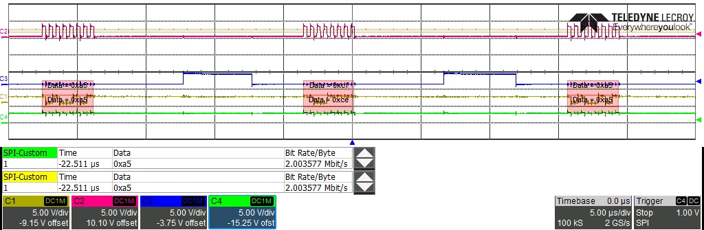
Can someone please point out or give helpful tips why this is not working as expected?

