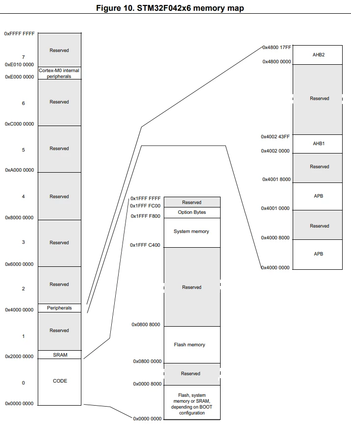
There is no special area, the only restriction is that the application vector table must be placed at 0x08000000, i.e. the lowest address in the flash, so you can't use page 0 for user data. The most straightforward way is to reserve the last pages of the flash for user data.
The flash is documented in chapter 3 of the reference manual, find the Flash memory organization table for your MCU there. Note the page size, pages are the units for erase operation, i.e. a whole page must be erased at one whenever you would like to overwrite data.
Find the linker script of your project (*.ld when using the gnu toolchain), and decrease the flash length parameter there. I have a STM32F030F4, the flash memory definition in my STM32F030F4PX_FLASH.ld reads
FLASH (rx) : ORIGIN = 0x8000000, LENGTH = 16K
the above mentioned table says I have 1K pages, so I could e.g. replace it with
FLASH (rx) : ORIGIN = 0x8000000, LENGTH = 13K
to reserve 3 pages. If you have an MCU with 2K pages, stick to even numbers.
Now the remaining area beyond the LENGTH value will never be touched by the linker, and your application is free to use it.
- You can't overwrite already programmed areas in flash with arbitrary values, only unused ones. To overwrite it, you must erase the whole page first.
- Overwriting a halfword with 0x0000 works.
- Note that the flash is not guaranteed to work after
1000 10000 erase operations.