

STM32CubeProgrammer: STM32H7A3xG Bank 2 address mismatch
Good afternoon,
We are working with STM32H7A3 boards and are currently migrating our build and flashing toolchain from STM32CubeIDE 1.9.0 to 2.2.0. During the migration we ran into a flash programming failure that we have traced to the device description, and we would like your confirmation before we adopt a workaround.
WHAT WE OBSERVE
Programming at 0x08100000 is rejected with "Operation exceeds memory limits" under 2.2.0. The same operation succeeded under 1.9.0.
Investigating this led to two findings on Device ID 0x480:
- STM32_Prog_DB_0x480.xml declares the Bank 2 base address for the 1 MB configuration as 0x08080000, which contradicts RM0455 Rev 13, Table 15, and consequently excludes the documented Bank 2 base at 0x08100000 from the valid range;
- Writes to 0x08080000 are accepted and verify successfully on our samples, despite Table 15 listing that range as not mapped.
FINDING 1 - DEVICE DESCRIPTION FILE
The file defines two configurations for Device ID 0x480, corresponding to the 2 MB and 1 MB flash variants:
| Configuration | Bank 1 | Bank 2 |
|---|---|---|
| config="0,1" (2 MB) | 0x08000000, occurrence 0x80 | 0x08100000, occurrence 0x80 |
| config="10,11" (1 MB) | 0x08000000, occurrence 0x40 | 0x08080000, occurrence 0x40 |
Sector size in both configurations: 0x2000 (8 KB).
Selection between them is driven by the flash size register. Configurations 0xA and 0xB in the JTAG_SWD interface block, that is, 10 and 11, the ones mapping to the 1 MB flash configuration, are gated on:
<ReadRegister address="0x08fff80c" mask="0x00000FFF" value="0x400"/>
Thus, a part reporting 0x400 (1024 KB) selects the 1 MB configuration, which defines Bank 2 at 0x08080000.
RM0455 Rev 13, Table 15 (Flash memory organization, STM32H7A3xG devices) specifies:
Bank 1: 0x08000000 - 0x0807FFFF, sectors 0-63
Bank 2: 0x08100000 - 0x0817FFFF, sectors 0-63
0x08080000 - 0x080FFFFF: not mapped
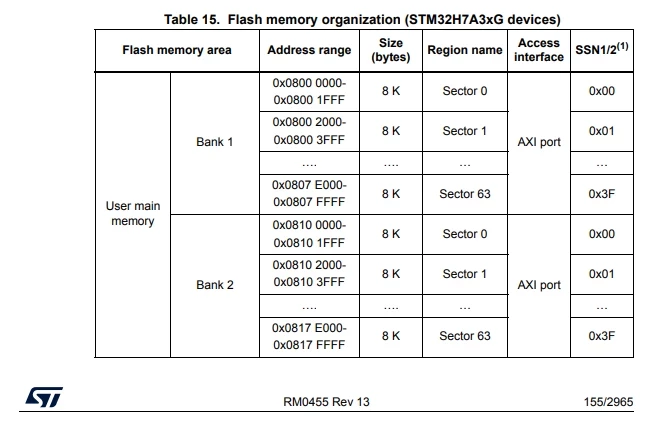
There is also an internal inconsistency in the same file. In the 2 MB configuration, the declared span size="0x200000" matches the sector fields exactly (0x80 x 0x2000 x 2 banks = 0x200000). In the 1 MB configuration the same value is declared:
<Parameters address="0x08000000" name="1 MBytes Dual Bank Embedded Flash" size="0x200000"/>
while the two sector fields there cover only 0x100000 bytes in total. With Bank 2 at 0x08080000, the sector definitions end at 0x080FFFFF, so the declared configuration span appears inconsistent with the actual address ranges defined by those fields.
STEPS TO REPRODUCE
- Connect to an STM32H7A3xG target (flash size register at 0x08FFF80C reports 0x400).
- Using CubeProgrammer as bundled with CubeIDE 2.2.0, program any data at 0x08100000.
Operation exceeds memory limits. - Program the same data at 0x08080000 instead.
Expected: the operation not to succeed.
Result: Programming and verification succeed.
The contrast between steps 2 and 3 is the core of this report: the only address range the reference manual documents as Bank 2 is refused, while an address the reference manual does not map is accepted.
FINDING 2 - BOTH ADDRESSES ARE PROGRAMMABLE
Under STM32CubeIDE 1.9.0, 0x08100000 was our default production flashing address. Devices programmed there boot and run correctly in the field. Under 2.2.0, which rejects 0x08100000 and resolves the 1 MB configuration to 0x08080000 instead, we programmed and verified at 0x08080000 on our samples, also successfully, but we are not assuming the behaviour generalises.
In our testing, both addresses accepted writes and passed verification, while RM0455 Table 15 maps only 0x08100000 as user main memory.
IMPACT AND VERSION BRACKET
Our project uses a dual-bank layout, following Table 15. CubeIDE 2.2.0 cannot program this layout through the device database as shipped. Since 1.9.0 programmed 0x08100000 without complaint, we assume the 1 MB configuration was introduced or modified somewhere between the CubeProgrammer releases bundled with 1.9.0 and 2.2.0. This may help narrow down where the change was introduced. We should add that we have traced the behaviour to the device description as the most likely source, but we are not in a position to rule out the internal flash loader as a contributing factor.
WORKAROUND
Editing the Bank 2 base address in the 1 MB configuration to 0x08100000 restores correct programming behaviour. We would rather not depend on this, since it is overwritten on every tool update.
REQUEST
- Please confirm whether RM0455 Table 15 or the device description file is authoritative for STM32H7A3xG, and correct whichever is in error.
- Please clarify how the 0x08080000 - 0x080FFFFF range decodes on STM32H7A3xG. In particular, is this range an alias or alternate address window for Bank 2, or does it correspond to a distinct physical Flash region? We need to know which bank the range belongs to, since that determines whether read-while-write applies between an image slot placed there and code executing from Bank 1.
If the range is not mapped and not supported, we accept that and will keep our layout at 0x08100000. In that case, however, the device description supplied with CubeProgrammer is directing users to program at an address that ST does not support, while writes to that address are accepted and verified rather than rejected. We would therefore ask you to treat this as the primary issue.
Our concern is that the tooling reports success throughout the entire programming and verification flow. A user following the address mapping presented by CubeProgrammer 2.2.0 could therefore program, verify, and ship a device with its secondary image slot located in a range that ST does not support, without any warning that the address is outside the documented Flash map.
Thank you,
José Cláudio