STM32C031C6 Timer confusion
The code below links Timer1 in master mode to Timer3 in slave mode producing a 4 second toggle on PB8 and it works correctly.
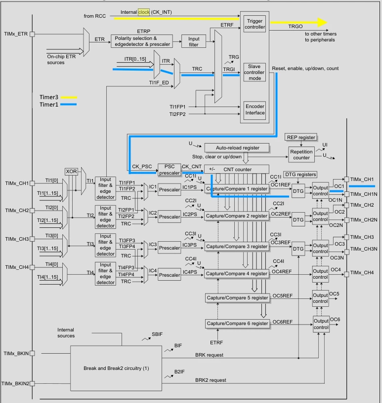
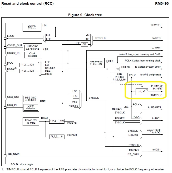
My question is I'm not able to follow the flow of the signal in the Timer chart below the code.
If someone would show me the signal flow I would appreciate it. I have shown how I think the signal flows. Is this correct?
void LinkTimer1And3()
{
// GPIOB clock enable
RCC->IOPENR = 2;
// Set PB8 alternate function
GPIOB->MODER &= ~(3 << 16);
GPIOB->MODER |= (2 << 16);
// Alternate function to TIM3 CH1
GPIOB->AFR[1] &= ~0x0f;
GPIOB->AFR[1] |= 3;
// Enable TIM1 and TIM3 clocks
RCC->APBENR2 |= (1 << 11);
RCC->APBENR1 |= (1 << 1);
// Master Mode Selection - Select Update Event as Trigger output (TRG0)
TIM1->CR2 |= (2 << 4);
// Slave Mode Control Register - Configure in slave mode using ITR1 as
// internal trigger. External Clock Mode 1 - Rising edges of the selected
// trigger (TRGI) clock the counter.
TIM3->SMCR |= 7;
// Set Prescaler and Auto Reload Register to slow the
// processor down so we can see the LED blink.
// Freq = 12MHz / ((12000 - 1) * (1000 - 1)) = 1Hz
TIM1->PSC = 12000 - 1;
TIM1->ARR = 1000 - 1;
TIM3->PSC = 0;
TIM3->ARR = 4 - 1;
// OC1M Toggle output
TIM3->CCMR1 |= (3 << 4);
// CC1E Enable output
TIM3->CCER |= 1;
// Master Output Enable
TIM3->BDTR |= (1 << 15);
TIM1->CR1 |= 1;
TIM3->CR1 |= 1;
while(1);
}