

STM32 external DAC sine wave problem.
Hi!
I would like to make a wav. player using STM32 microcontroller. My first step was to generate a sine wave using STM32F103C8T6, SPI interface and external DAC MCP4921. However, it's not working.
I attach the schematic of my device.
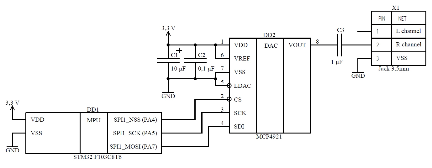
I wrote 2 versions of my program using CMSIS in STM32CubeIDE. In the first version of the program a timer is generating an interrupt every second. Every 4 seconds microcontroller sends a digital value to the external DAC using SPI interface. I checked the output of the DAC with multimeter and voltage levels are correct. It is working. I also checked RCC, GPIO, SPI and timer blocks of microcontroller: they all work. So, the first version of the program works perfectly.
In the second version of the program a buffer is initialised with 100 sine wave values. A timer is generating an interrupt with a frequency of 40kHz, microcontroller sends a sine value to the external DAC using SPI interface. The frequency of the sine wave should be 400Hz. However, I cant hear a correct tone when I plug in my headphones. I also cant see anything when I plug the signal to the virtual oscilloscope through the microphone input of my computer (unfortunately I don't have an oscilloscope). When I change the sampling frequency (interrupt frequency of the timer) I either dont hear anything or hear some disturbing gibberish.
Appreciate your help.
//#include "main.h"
#include "stm32f1xx.h"

void RCCinit(void);
void GPIOinit(void);
void SPIinit(void);
void SPItransmit(unsigned int data);
void TIMinit(void);

unsigned int i=0;

unsigned int buf[100]=
{
		620,659,698,736,774,812,848,884,919,952,
		984,1015,1044,1072,1098,1122,1143,1163,1181,1196,
		1210,1221,1229,1235,1239,1240,1239,1235,1229,1221,
		1210,1196,1181,1163,1143,1122,1098,1072,1044,1015,
		984,952,919,884,848,812,774,736,698,659,
		620,581,542,504,466,428,392,356,321,288,
		256,225,196,168,142,118,97,77,59,44,
		30,19,11,5,1,0,1,5,11,19,
		30,44,59,77,97,118,142,168,196,225,
		256,288,321,356,392,428,466,504,542,581
};

int main (void)
{
	RCCinit();
	GPIOinit();
	SPIinit();
	TIMinit();

	while(1)
	{

	}
}

void RCCinit(void)
{
	FLASH->ACR|=FLASH_ACR_PRFTBE; //Prefetch is enabled.
	while(!(FLASH->ACR&FLASH_ACR_PRFTBS)); //Prefetch buffer is disabled.
	FLASH->ACR&=~FLASH_ACR_HLFCYA; //Half cycle is disabled.
	FLASH->ACR&=~FLASH_ACR_LATENCY;
	//FLASH->ACR|=FLASH_ACR_LATENCY_0; //One wait state, if 24 MHz < SYSCLK ≤ 48 MHz
	FLASH->ACR|=FLASH_ACR_LATENCY_1; //Two wait states, if 48 MHz < SYSCLK ≤ 72 MHz.


	RCC->CR|=RCC_CR_HSEON; //HSE oscillator ON. 8MHz.
	while(!(RCC->CR&RCC_CR_HSERDY)); //HSE oscillator not ready.

	RCC->CFGR&=~RCC_CFGR_PLLXTPRE; //HSE clock not divided. 8MHz.
	RCC->CFGR|=RCC_CFGR_PLLSRC; //HSE oscillator clock selected as PLL input clock.
	RCC->CFGR&=~RCC_CFGR_PLLMULL;
	RCC->CFGR|=RCC_CFGR_PLLMULL9; //PLL input clock x 9. 72MHz.
	RCC->CFGR&=~RCC_CFGR_HPRE; //SYSCLK not divided.
	RCC->CFGR&=~RCC_CFGR_PPRE1;
	RCC->CFGR|=RCC_CFGR_PPRE1_DIV2; //HCLK divided by 2. 36MHz.
	RCC->CFGR&=~RCC_CFGR_PPRE2; //HCLK not divided.
	RCC->CFGR&=~RCC_CFGR_USBPRE; //PLL clock is divided by 1.5. 48MHz.

	RCC->CR|=RCC_CR_PLLON; //PLL ON.
	while(!(RCC->CR&RCC_CR_PLLRDY)); //PLL unlocked.
	RCC->CFGR&=~RCC_CFGR_SW;
	RCC->CFGR|=RCC_CFGR_SW_PLL; //PLL selected as system clock.
	while(!(RCC->CFGR&RCC_CFGR_SWS_PLL)); //PLL used as system clock.


	RCC->APB1ENR|=RCC_APB1ENR_TIM2EN; //TIM2 timer clock enable.
	RCC->APB2ENR|=RCC_APB2ENR_IOPCEN|RCC_APB2ENR_IOPAEN|RCC_APB2ENR_AFIOEN|RCC_APB2ENR_SPI1EN; //IO port C, IO port A, Alternate function I/O, SPI 1 clock enabled.
}

void GPIOinit(void)
{
	//SPI pins.
	GPIOA->CRL|=GPIO_CRL_MODE4|GPIO_CRL_MODE5|GPIO_CRL_MODE7; //Output mode, max speed 50 MHz.
	GPIOA->CRL&=~(GPIO_CRL_CNF4|GPIO_CRL_CNF5|GPIO_CRL_CNF7);
	GPIOA->CRL|=GPIO_CRL_CNF4_1|GPIO_CRL_CNF5_1|GPIO_CRL_CNF7_1; //Alternate function output Push-pull.

	//C13
	GPIOC->CRH|=GPIO_CRH_MODE13; //Output mode, max speed 50 MHz.
	GPIOC->CRH&=~GPIO_CRH_CNF13; //General purpose output push-pull.
	GPIOC->ODR|=GPIO_ODR_ODR13;
}

void SPIinit(void)
{
	SPI1->CR1&=~SPI_CR1_BR;
	SPI1->CR1|=SPI_CR1_BR_0; //fPCLK/4=72MHz/4=18MHz.
	SPI1->CR1&=~(SPI_CR1_CPOL|SPI_CR1_CPHA); //CK to 0 when idle. The first clock transition is the first data capture edge.
	SPI1->CR1|=SPI_CR1_DFF; //16-bit data frame format is selected for transmission/reception.
	SPI1->CR1&=~SPI_CR1_LSBFIRST; //MSB transmitted first.
	SPI1->CR1&=~(SPI_CR1_SSM|SPI_CR1_SSI); //Software slave management disabled.
	SPI1->CR2|=SPI_CR2_SSOE; //SS output is enabled in master mode and when the cell is enabled. The cell cannot work in a multimaster environment.

	SPI1->CR1&=~(SPI_CR1_BIDIMODE|SPI_CR1_RXONLY); //2-line unidirectional data mode selected. Full duplex (Transmit and receive).
	SPI1->CR1&=~SPI_CR1_CRCEN; //CRC calculation disabled.
	SPI1->CR2&=~(SPI_CR2_TXEIE|SPI_CR2_RXNEIE|SPI_CR2_ERRIE|SPI_CR2_TXDMAEN|SPI_CR2_RXDMAEN); //TXE, RXNE, Error interrupt is masked. Tx, Rx buffer DMA disabled.

	SPI1->I2SCFGR&=~SPI_I2SCFGR_I2SMOD; //SPI mode is selected.

	SPI1->CR1|=SPI_CR1_MSTR; //Master configuration.
}

void SPItransmit(unsigned int data)
{
	SPI1->CR1|=SPI_CR1_SPE; //Peripheral enabled.
	while(!(SPI1->SR&SPI_SR_TXE)); //Tx buffer not empty.
	SPI1->DR=0x7000U|(data&0xFFFU);
	while(!(SPI1->SR&SPI_SR_TXE)); //Tx buffer not empty.
	while(SPI1->SR&SPI_SR_BSY); //SPI (or I2S) is busy in communication or Tx buffer is not empty.
	SPI1->CR1&=~SPI_CR1_SPE; //Peripheral disabled.
}

void TIMinit(void)
{
	//fapb1=36MHz. fclk=36*2=72MHz.
	TIM2->CR1&=~TIM_CR1_UDIS; //UEV enabled.
	TIM2->CR1&=~TIM_CR1_URS; //Any of the following events generate an update interrupt or DMA request if enabled. These events can be: – Counter overflow/underflow. – Setting the UG bit. – Update generation through the slave mode controller.
	TIM2->CR1&=~TIM_CR1_OPM; //Counter is not stopped at update event.
	TIM2->CR1&=~TIM_CR1_DIR; //Counter used as upcounter.
	TIM2->CR1&=~TIM_CR1_CMS; //Edge-aligned mode.
	TIM2->CR1|=TIM_CR1_ARPE; //TIMx_ARR register is buffered.
	TIM2->CR1&=~TIM_CR1_CKD; //tDTS = tCK_INT.
	TIM2->DIER|=TIM_DIER_UIE; //Update interrupt enabled.
	NVIC_EnableIRQ(TIM2_IRQn);
	TIM2->PSC=17; //Prescaler value.
	TIM2->ARR=99; //Auto-reload register. fUEV=72MHz/()=Hz.
	TIM2->CNT=0; //Counter value.
	TIM2->CR1|=TIM_CR1_CEN; //Counter enabled.
}

void TIM2_IRQHandler(void)
{
	//C13 мигает
	//GPIOC->ODR^=GPIO_ODR_ODR13;

	if(i==100)
	{
		i=0;
	}
	SPItransmit(buf[i]);
	i++;

	TIM2->SR&=~TIM_SR_UIF; //Update interrupt flag. It is cleared by software. No update occurred.
}