

Question
SPI full duplex not working, but MOSI and MISO lines work fine individually. How do I fix this?
Pardon me for asking repeated questions on SPI, but it's giving me a lot of issues. So far I have configured two STM32 boards as master and slave, and ran code for MOSI and MISO lines individually which seemed to work fine. Now that I combine those codes for full duplex communication, I am getting wrong data.
Assume all functions called work correctly.
Master code :
#include "stm32l4xx.h" // Device header
#include <string.h>

#define CS_LOW (GPIOA->BSRR = (1<<20))
#define CS_HI (GPIOA->BSRR = (1<<4))


void SPI_init(void);
void SPI_write(uint8_t data);
void SPI_writestring(char* str);
void delayms(int count);
void setclkfreq(void);

void UART_init(void);
void uart_txchar(char c);
void uart_txstr(char* string);


int main()
{
	char buff[16] = {0};
	setclkfreq();						//set clock to 16Mhz

	SPI_init();
	UART_init();

	CS_HI;

	while(1)
	{
		//MOSI

		CS_LOW;
		SPI_writestring("Execute");
		CS_HI;

		delayms(1);

		//*********************************************************
		//MISO

		CS_LOW;

		for(int i=0; i<12; i++)
		{
			SPI_write(0x00);					//write dummy byte
			buff[i] = *(__IO uint8_t *)&SPI1->DR;				//store MISO data in buff
		}

		CS_HI;

		uart_txstr(buff);
		uart_txstr("\n\r");

		delayms(500);
	}

}


void SPI_init(void)
{
	RCC->AHB2ENR |= RCC_AHB2ENR_GPIOAEN;

	RCC->APB2ENR |= RCC_APB2ENR_SPI1EN;

	GPIOA->MODER &=~(3<<8 | 3<<10 | 3<<12 | 3<<14);
	GPIOA->MODER |= (1<<8 | 2<<10 | 2<<12 | 2<<14);			//CS is selected as GPO while others are AFs

	//GPIOA->PUPDR |= 1<<12;			//pull up MISO line


	GPIOA->AFR[0] &=~(0XF<<20 | 0xF<<24 | 0xF<<28);
	GPIOA->AFR[0] |= (5<<20 | 5<<24 | 5<<28);				//af for mosi,miso and sck

	SPI1->CR1 &=~ (SPI_CR1_SPE);
	SPI1->CR1 |= (3<<3) | SPI_CR1_MSTR | SPI_CR1_SSI | SPI_CR1_SSM;

	SPI1->CR1 |= SPI_CR1_SPE;
}


void SPI_write(uint8_t data)
{
	*(__IO uint8_t *)&SPI1->DR = data;
	while(!(SPI1->SR & SPI_SR_TXE));
	while((SPI1->SR & SPI_SR_BSY));

}


void SPI_writestring(char* str)
{
	int len = strlen(str);

	for(int i=0; i<len; i++)
	{
		//CS_LOW;
		SPI_write(str[i]);
		//CS_HI;
	}

}


void delayms(int count)
{
	int i;
	SysTick->LOAD = 16000;		//16000 cycles in 1 ms
	SysTick->VAL = 0;					//reset current value to 0
	SysTick->CTRL = 5;				//clksource = internal. counter enabled. interrupt disabled

	for(i=0; i<count; i++)			//repeat 1ms cycles count number of times
	{
		while((SysTick->CTRL & 0x10000)==0){}			//do nothing till Countflag becomes 1
	}

	SysTick->CTRL=0;		//disable counter

}


void setclkfreq(void)
{
	FLASH->ACR &=~ FLASH_ACR_LATENCY;
	FLASH->ACR |= FLASH_ACR_LATENCY_0WS;

	RCC->CR |= RCC_CR_MSION;		//turn on MSI (Multi Speed Internal)

	RCC->CFGR &=~ RCC_CFGR_SW;

	while(!(RCC->CR & RCC_CR_MSIRDY));

	RCC->CR &=~ RCC_CR_MSIRANGE;
	RCC->CR |= RCC_CR_MSIRANGE_8;				//16Mhz

	RCC->CR |= RCC_CR_MSIRGSEL;

	while(!(RCC->CR & RCC_CR_MSIRDY));


}

void UART_init(void)
{
	RCC->APB1ENR1 &=~ RCC_APB1ENR1_USART2EN;
	RCC->APB1ENR1 |= RCC_APB1ENR1_USART2EN;		//ENABLE UART2

	RCC->AHB2ENR &=~ RCC_AHB2ENR_GPIOAEN;
	RCC->AHB2ENR |= RCC_AHB2ENR_GPIOAEN;			//PORT A enable


	GPIOA->AFR[0] &=~ 0XF00;
	GPIOA->AFR[0] |= 0X700;				//ENABLE transmit

	GPIOA->MODER &=~(3<<4);
	GPIOA->MODER |= 2<<4;			//PA2 output

	USART2->CR1 &=~ (USART_CR1_UE);

	USART2->BRR = 0x683;				// 9600 bps

	USART2->CR1 |= USART_CR1_TE;

	USART2->CR1 |= USART_CR1_UE;

}

void uart_txchar(char c)
{
	while(!(USART2->ISR & (USART_ISR_TXE)));
	USART2->TDR = c;
	while(!(USART2->ISR & USART_ISR_TC));

}

void uart_txstr(char* string)
{
	while(*string)
	{
		uart_txchar(*(string++));
	}

}
Slave side code:
#include "stm32f4xx.h" // Device header
#include <string.h>

/*
PA5 - SCK
PA4 - NSS
PA7 -MOSI
PA6 - MISO
*/


#define CS_HI (GPIOA->ODR |= 1<<4)
#define CS_LOW (GPIOA->ODR &=~(1<<4))


void SPI1_init(void);
char SPI_read(void);
void delayms(int count);
void uart_txchar(char c);
char uart_rx(void);
void UART_init(void);
void uart_txstr(char* string);

void SPI_write(char data);
void SPI_writestring(char* str);


int main()
{

	char buff[16] = {0};
	char c;
	UART_init();
	SPI1_init();

	while(1)
	{
		//MOSI
		uart_txstr("\n\rReceived : ");


		for(int i=0; i<7; i++)
		{
			buff[i] = SPI_read();
		}

		uart_txstr(buff);

		delayms(1);

		//***********************************************************
		//MISO
		SPI_writestring("Acknowledged");
		delayms(500);

	}

}


void SPI1_init(void)
{
	RCC->AHB1ENR |= RCC_AHB1ENR_GPIOAEN;								//enable clock to PortA

	RCC->APB2ENR |= RCC_APB2ENR_SPI1EN;						//enable clock to SPI1

	GPIOA->MODER &= ~(3<<14 | 3<<10 | 3<<12 | 3<<8);		//clear SPI bits
	GPIOA->MODER |= (2<<10 | 2<<14 | 2<<12 | 2<<8 );	//set MOSI,MISO,NSS,SCK bits for AF

	GPIOA->PUPDR |= 1<<14;
	//GPIOA->PUPDR |= 2<<12;				//pull down miso

	GPIOA->AFR[0] &= ~(0xF<<16 | 0xF<<20 | 0xF<<24 | 0xF<<28);			//clear AF
	GPIOA->AFR[0] |= (5<<20 | 5<<24 | 5<<28 | 5<<16);			//setting AF05 for MOSI,MISO and SCK

	SPI1->CR1 &=~(SPI_CR1_SPE);
	SPI1->CR1 |= (3<<3);											//Mode0
	SPI1->CR1 &=~ (SPI_CR1_MSTR | SPI_CR1_SSI | SPI_CR1_SSM);

	SPI1->CR1 |= SPI_CR1_SPE;										//SPI enable

}


char SPI_read(void)
{
	char data;
	while(!(SPI1->SR & SPI_SR_RXNE));


	while(SPI1->SR & SPI_SR_BSY);

	data = SPI1->DR;

	return data;

}

void SPI_write(char data)
{
	SPI1->DR = data;

	while(!(SPI1->SR & SPI_SR_TXE));
	while(SPI1->SR & SPI_SR_BSY);
}

void SPI_writestring(char* str)
{
	int len= strlen(str);

	for(int i=0; i<len; i++)
	{
		SPI_write(str[i]);
	}
}


void delayms(int count)
{
	int i;
	SysTick->LOAD = 16000;		//16000 cycles in 1 ms
	SysTick->VAL = 0;					//reset current value to 0
	SysTick->CTRL = 5;				//clksource = internal. counter enabled. interrupt disabled

	for(i=0; i<count; i++)			//repeat 1ms cycles count number of times
	{
		while((SysTick->CTRL & 0x10000)==0){}			//do nothing till Countflag becomes 1
	}

	SysTick->CTRL=0;		//disable counter

}


void uart_txchar(char c)
{
	while((USART2->SR & (1<<7))==0);
	USART2->DR = (c);
}

char uart_rx(void)
{
	char c;
	while((USART2->SR & 1<<5)==0);		//while RXNE ==0 (data not received) don't do anything
	c = (USART2->DR);
	return c;
}

void uart_txstr(char* string)
{
	while(*string)
	{
		uart_txchar(*(string++));
	}

}

void UART_init(void)
{
	RCC->APB1ENR |= 1<<17;			//USART2 clock enable
	RCC->AHB1ENR |= 1;			//Port A clock enable
	GPIOA->AFR[0] |= 0x7700;		//GPIOA AF7 = USART2, portA2 and PORTA3 have UART afs
	GPIOA->MODER |=1<<5 | 1<<7;


	USART2->BRR = 0X683;
	USART2->CR1 |= 1<<3 | 1<<2; 				//TX Enable RX enable
	USART2->CR1 |= 1<<13;			//UART enable
}

void delayus(int count)
{
	int i;
	SysTick->LOAD = 16;		//4000 cycles in 1 ms
	SysTick->VAL = 0;					//reset current value to 0
	SysTick->CTRL = 5;				//clksource = internal. counter enabled. interrupt disabled

	for(i=0; i<count; i++)			//repeat 1ms cycles count number of times
	{
		while((SysTick->CTRL & 0x10000)==0){}			//do nothing till Countflag becomes 1
	}

	SysTick->CTRL=0;		//disable counter
}

void dma_spi_read(char* buff)
{
	RCC->AHB1ENR |= RCC_AHB1ENR_GPIOAEN | RCC_AHB1ENR_DMA2EN;								//enable clock to PortA
	RCC->APB2ENR |= RCC_APB2ENR_SPI1EN;						//enable clock to SPI1


	SPI1->CR2 |= SPI_CR2_RXDMAEN;

	//DMA2 , Stream2 Channel 3
	DMA2_Stream2->CR |= 3<<25 | DMA_SxCR_CIRC | DMA_SxCR_TCIE | DMA_SxCR_MINC ;

	DMA2_Stream2->NDTR = 7;

	DMA2_Stream2->PAR = (uint32_t)&SPI1->DR;

	DMA2_Stream2->M0AR = (uint32_t)buff;


	//SPI1->CR1 &= ~(1<<6);
	SPI1->CR1 &=~(SPI_CR1_SPE);
	SPI1->CR1 |= (3<<3);											//Mode0
	//SPI1->CR1 &=~(1<<11);
	//SPI1->CR2 |= 0;												//Motorola Frame format
	SPI1->CR1 |= SPI_CR1_SPE;										//SPI enable

	GPIOA->MODER &= ~(3<<14 | 3<<10 | 3<<12 | 3<<8);		//clear SPI bits
	GPIOA->MODER |= (2<<10 | 2<<14 | 2<<12 | 2<<8 );	//set MOSI,MISO,SCK bits for AF and NSS as GPO

	GPIOA->PUPDR |= 1<<14;

	GPIOA->AFR[0] &= ~(0xF<<20 | 0xF<<24 | 0xF<<28);			//clear AF
	GPIOA->AFR[0] |= (5<<20 | 5<<24 | 5<<28 | 5<<16);			//setting AF05 for MOSI,MISO and SCK

}
If I run the code on either side of "**************" line individually it works correctly, I get the correct string on PC terminal.
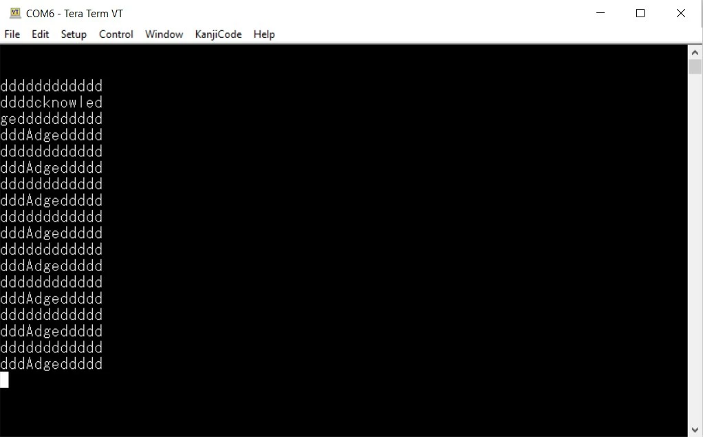
But with the code shown above, this is what I get
On master side:
On slave side:
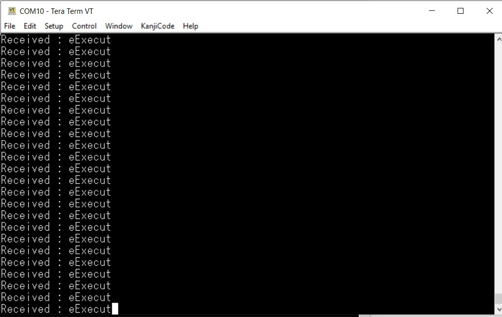
The slave side seems to be receiving it somewhat correctly, while the master is receiving absolutely wrong message.
What I am doing wrong?
