

Albi G.
Associate III
June 11, 2020
Question

QUAD-SPI too busy!

  • June 11, 2020
  • 21 replies
  • 8968 views

Hi guys,

i am using the QuadSPI periphery to interface with a FPGA. I am in need of raw throughput with alternating write and read cycles of some number of bytes. I am just concept-prooving right now.

Since QUADSPI->CCR is not allowed to be modified when BUSY==1 the busy flag effectively limits the command rate - which is useful since i obviously need to wait to finish a a command before sending the next one.

My configuration is:

  • 4 bit wide Instruction
  • Skip directly to 4bit wide Data-transfer
  • Min CS-High time = 0 (1 cycle)
  • IndirectRead / IndirectWrite mode, no DMA for now.

Now, unfortunately the BUSY flag is rather lame and it takes exactly 6-7 clocks after CS rises that the BUSY flag clears. That is really **** ** the achievable command rate!

With 6-7 clocks, i mean periphery-clocks after the prescaler. (@1MHz SPI clock, the BUSY-signal is 1 for 6µs after CS rises. If 10MHz is used, then its 0.6us)

What i dont understand is, that this behavior makes the minimum CS-high setting kind of useless. (i never achieve a scenario where CS is less than 6 cycles high in-between commands)

This holds true for consecutive reads, consecutive writes, and alternating read-write.

What could go wrong ??

This is my example code. Not using the library, but my code hopefully reads kind of intuitively...
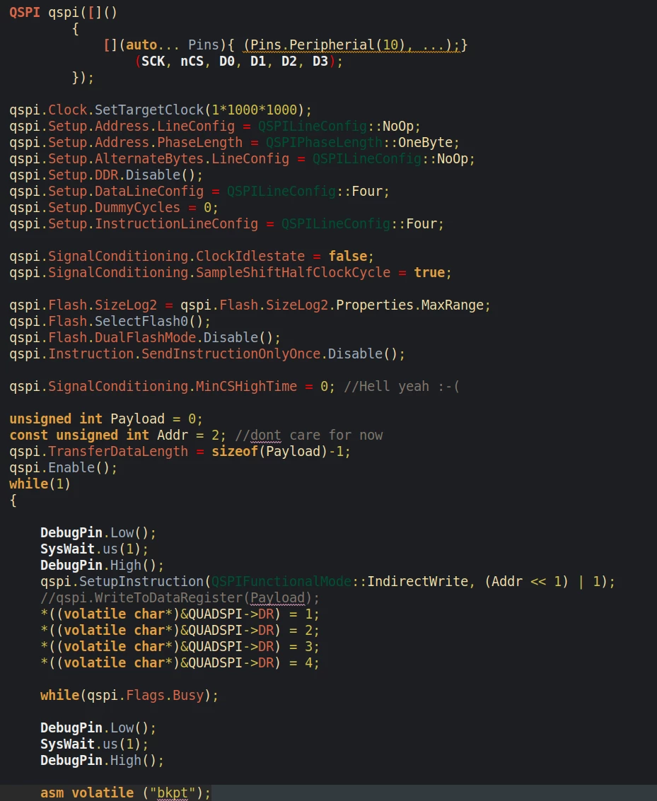

_legacyfs_online_stmicro_images_0693W000001qTAI.png

Measured though my Debug-GPIO: 16.7µs from Command start to BUSY=0

Chip select Low for 11µs

Give me a faster BUSY, please :(

BTW: i also get the same behavior if i configure the QSPI differently:

  • skip Instruction
  • Send one byte address
  • skip directly to Data

== Same timing(-problems)

thanks

This topic has been closed for replies.

21 replies

Andreas Bolsch
Lead III
June 11, 2020

There is nothing wrong, but only a misconception regarding the design goal of the QSPI. From the RM: "The QUADSPI is a specialized communication interface targeting single, dual or quad SPI Flash memories. ...". One might add: "For anything else, your mileage may vary." The whole chapter in the RM deals only with attaching flash memory, that is clear enough.

For the intended use, it's the performance in memory mapped mode which really matters. Indirect read/write are intended for programming the flash (this includes status read, write enabling, ...). This is inherently quite slow, hence e.g. command startup time (or in your case return to idle state) doesn't matter that much when a whole page is sent to the flash in a single operation and then the chip has to be polled until programming has finished.

CSHT is certainly relevant only in memory mapped mode.

In your case, the FMC or PSSI (on H7A/B) might be a feasible option, except that if you intend to use only 4-bit parallel data, the necessary packing/unpacking might be an obstacle.

Albi G.
Albi G.Author
Associate III
June 11, 2020

So this is more a Quad-cripple instead a Quad-SPI?

The memory mapped mode is read-only which is totally useless for me :( One cant use SRAMs or FRAMs in QSPI-memory mapped mode.

There shouldnt be a conceptual reason for this behavior besides the intented purpose. This seems really just a faulty/lazy implementation of the hardware state machine. I mean, if BUSY=1 there must be something busy actually. What is it?

Unfortunately my package does not have the FMC and i cant really switch chips due to price and board space.

The quad-SPI should be really just a quad-spi. nothing more. This is frustrating. I appreciate the command configuration on top of that, but not when it is so crippling.

My intented purpose was to use the QSPI as a high throughput device.

I have all 5 ADCs running at full speed. I use DMA to put the results next to each other in memory and after that, another DMA should be triggered to write those values to QSPI which is attached to an FPGA/coprocessor. After the QSPI-write-DMA finishes, the results must be read back via DMA.

All my plans ruined.

!!UNDOCUMENTED!!

Andreas Bolsch
Lead III
June 11, 2020

Sorry for the bad news ...

You might try not to wait for BUSY to be reset but instead for TCF becoming set and then set ABORT right away. This might save a few cycles, but I doubt it will be fast enough for your purpose.

Albi G.
Albi G.Author
Associate III
June 11, 2020

Tried that, TCF and BUSY are one and the same for this purpose. Same useless 6 cycle delay.

berendi
Principal
June 11, 2020

Please post the contents of the QSPI registers before and after issuing the command.

Albi G.
Albi G.Author
Associate III
June 11, 2020

Easy enough.

This is the initialization-code and the lop that just fills the FIFO. This results in 1 Instruction + 1 Data Byte (4clks) + 6 useless waiting clocks

0693W000001qXYOQA2.png

The QUAD-SPI is filled with what is down below. This is read with debugger at the bkpt-insturction:

QUADSPI->CR = 0xa6000011;
QUADSPI->DCR = 0x1f0000;
//QUADSPI->SR = 4;
//QUADSPI->FCR = 0;
QUADSPI->CCR = 0x3000301;
QUADSPI->AR = 0;
QUADSPI->ABR = 0;
//QUADSPI->DR = 0;
QUADSPI->PSMKR = 0;
QUADSPI->PSMAR = 0;
QUADSPI->PIR = 0;
QUADSPI->LPTR = 0;

 I am not sure what "after the command" means in that context. There is "no after the command" here, its "instantaneous" restart since data is available and that is what triggers a transfer as per datasheet..... after 6 idle qspi clocks.

Arnon
Associate III
June 11, 2020

Hi @Albi G.​ 

I don't have answers to your question

but I share your frustration

I am trying to do the same: use the QSPI for FPGA communication. using indirect mode, data phase only.

My problem with the busy bit that sometime it will stay "set" forever (interface is not active)

--Arnon

Andreas Bolsch
Lead III
June 11, 2020

If you refer to indirect read mode: That's a known bug on the H753 etc., see errata sheet, 2.5.3. As the QSPI interface seems to almost identical across the various devices, I wouldn't be surprised if this is present on other devices as well.

Arnon
Associate III
June 11, 2020

thank you @Andreas Bolsch​ 

Yes, I do refer to  indirect read mode.

the errata state "slave mode" while I have configured the CPU to be the master.

I am using HAL_QSPI_Receive_DMA(&hqspi,(buffer) to trigger read.

--Arnon

berendi
Principal
June 12, 2020

I've played with it a bit on a STM32H743 (I don't have any STM32G4), the only difference is that BUSY is cleared after 5 cycles instead of 6.

The only way to cut it short is to reset it in the RCC. But then you have to reload all of the QSPI registers.

I have a vague idea working proof of concept below how it could be done quickly without software intervention.

berendi
Principal
June 15, 2020

So the basic idea is to reset QUADSPI in the RCC, then reprogram its registers as their contents are lost at reset. All of it is handled by timers and DMA autonomously.

static uint32_t qspireset[] = { RCC_AHB3RSTR_QSPIRST, 0 };
	static uint32_t qspi_init_reg[6] = {
			(249 << QUADSPI_CR_PRESCALER_Pos) |
			QUADSPI_CR_SSHIFT |
			QUADSPI_CR_EN, // CR
 
			(0x1F << QUADSPI_DCR_FSIZE_Pos) |
			(0 << QUADSPI_DCR_CSHT_Pos), // DCR
 
			0, // SR
			0, // FCR
			0, // DLR
 
			QUADSPI_CCR_DMODE |
			(0 << QUADSPI_CCR_DCYC_Pos) |
			QUADSPI_CCR_IMODE |
			(1 << QUADSPI_CCR_INSTRUCTION_Pos) // CCR
	};
 
	// Copy a word from a memory variable (make sure it does not end up in DTCM)
	// to a RCC reset register. Circular mode, so the operation is repeated on every DMA request
	DMA1_Stream0->M0AR = (uint32_t)qspireset;
	DMA1_Stream0->PAR = (uint32_t)&RCC->AHB3RSTR;
	DMA1_Stream0->NDTR = 1;
	DMA1_Stream0->CR =
			DMA_SxCR_MSIZE_1 | // 10: 32 bit
			DMA_SxCR_PSIZE_1 | // 10: 32 bit
			DMA_SxCR_CIRC |
			DMA_SxCR_DIR_0 | // 00: P->M, 01:M->P, 10:M->M
			DMA_SxCR_EN;
 
	// same as above, different value
	DMA1_Stream1->M0AR = (uint32_t)(qspireset + 1);
	DMA1_Stream1->PAR = (uint32_t)&RCC->AHB3RSTR;
	DMA1_Stream1->NDTR = 1;
	DMA1_Stream1->CR =
			DMA_SxCR_MSIZE_1 | // 10: 32 bit
			DMA_SxCR_PSIZE_1 | // 10: 32 bit
			DMA_SxCR_CIRC |
			DMA_SxCR_DIR_0 | // 00: P->M, 01:M->P, 10:M->M
			DMA_SxCR_EN;
 
	// Copy 6 words from the initialization array to the QUADSPI registers
	DMA1_Stream2->M0AR = (uint32_t)&qspi_init_reg;
	DMA1_Stream2->PAR = (uint32_t)QUADSPI;
	DMA1_Stream2->NDTR = 6;
	DMA1_Stream2->CR =
			DMA_SxCR_MSIZE_1 | // 10: 32 bit
			DMA_SxCR_PSIZE_1 | // 10: 32 bit
			DMA_SxCR_PINC |
			DMA_SxCR_MINC |
			DMA_SxCR_CIRC |
			DMA_SxCR_DIR_0 | // 00: P->M, 01:M->P, 10:M->M
			DMA_SxCR_EN;
 
	DMAMUX1_Channel0->CCR = (DMA_REQUEST_TIM2_CH2 << DMAMUX_CxCR_DMAREQ_ID_Pos);
	DMAMUX1_Channel1->CCR = (DMA_REQUEST_TIM2_CH3 << DMAMUX_CxCR_DMAREQ_ID_Pos);
	DMAMUX1_Channel2->CCR = (DMA_REQUEST_TIM3_CH1 << DMAMUX_CxCR_DMAREQ_ID_Pos);
 
	// TIM3 triggers DMA1_Stream2 writes to the QUADSPI configuration registers.
	// It is gated by the TIM2_CH1 PWM output signal. When I tried reducing the
	// period to 10 cycles (ARR=9), DMA has started dropping requests. Perhaps because
	// DMA is on the AHB bus matrix, but both its source and destination must be
	// accessed through the AHB-AXI gateaway (and I did not bother with relocating
	// data to AHB SRAM). Should be a non-issue on the STM32G4,
	// so it might work with shorter periods there.
	TIM3->ARR = 19;
	TIM3->CCR1 = 5;
	TIM3->DIER = TIM_DIER_CC1DE;
	TIM3->SMCR =
			TIM_SMCR_TS_0 | // ITR1 = TIM2_TRGO
			TIM_SMCR_SMS_2|TIM_SMCR_SMS_0; // gated mode
 
	// TIM2 is started in one-pulse mode triggered by a rising edge on its ETR pin
	// which must be externally connected to QUADSPI NCS.
	// It triggers two DMA transfers first (on CH2 and CH3), setting and resetting
	// the QUADSPI reset bit in RCC.
	// Then it generates a pulse internally on CH1 (OC1REF) which gates TIM3.
	// The length of the pulse should be exactly 6 times the period of TIM3, i.e.
	// (TIM2->ARR + 1 - TIM2->CCR1) = 6 * (TIM3->ARR + 1), while TIM2->ARR is
	// roughly the time NCS stays high.
	TIM2->ARR = 199u;
	TIM2->CCR1 = 80u;
	TIM2->CCR2 = 1u;
	TIM2->CCR3 = 2u;
	TIM2->CCMR1 =
			TIM_CCMR1_OC1M_2|TIM_CCMR1_OC1M_1|TIM_CCMR1_OC1M_0; // TIM2_CH1 PWM mode 2
	TIM2->DIER = TIM_DIER_CC2DE | TIM_DIER_CC3DE; // CH2 and CH3 trigger DMA on compare event
	TIM2->SMCR =
			TIM_SMCR_TS_2|TIM_SMCR_TS_1|TIM_SMCR_TS_0 | // ETRF -> trigger input
			TIM_SMCR_SMS_2|TIM_SMCR_SMS_1; // trigger counter start
	TIM2->CR2 = (0b100u << TIM_CR2_MMS_Pos); // OC1REF -> TRGO
 
	// Enable TIM3, it would still wait for the gate signal to start counting
	TIM3->CR1 = TIM_CR1_CEN;
	// TIM2 will be enabled by ETR
	TIM2->CR1 = TIM_CR1_OPM;
 
	// Set up QUADSPI for the first transfer
	QUADSPI->DCR =
			(0x0F << QUADSPI_DCR_FSIZE_Pos) |
			(0 << QUADSPI_DCR_CSHT_Pos) |
			0;
	QUADSPI->CR = // 0xa6000011;
			(249 << QUADSPI_CR_PRESCALER_Pos) |
			//QUADSPI_CR_SSHIFT |
			QUADSPI_CR_EN;
	QUADSPI->DLR = 0;
	QUADSPI->CCR = // 0x03000301;
			QUADSPI_CCR_DMODE |
			(0 << QUADSPI_CCR_DCYC_Pos) |
			QUADSPI_CCR_IMODE |
			(1 << QUADSPI_CCR_INSTRUCTION_Pos);
	
	*(uint8_t *)&QUADSPI->DR = 1;
 
	// Wait for the QUADSPI BUSY flag to clear, shortly after it sets NCS high
	// the reset through RCC clears all status flags.
	while(QUADSPI->SR & QUADSPI_SR_BUSY)
		;
	// Wait for the timers to finish reinitializing the QUADSPI registers.
	// 
	while(TIM2->CR1 & TIM_CR1_CEN)
		;
 
	// Now QUADSPI is ready to transmit the next data packet.
	*(uint8_t *)&QUADSPI->DR = 1;

Of course you don't have to busy-wait for the timer to stop, either a timer DMA request on the update event or a QUADSPI DMA request could load the next value in the QUADSPI data register.

Apparently the STM32H7 DMA can't copy from peripheral to peripheral registers, so I had to use two DMA channels for that. The STM32G4 DMA should be able to do that, so you can do something like this

DMA1_Stream0->M0AR = (uint32_t)&TIM2->DMAR;
DMA1_Stream0->PAR = (uint32_t)&RCC->AHB3RSTR;
DMA1_Stream0->NDTR = 2;
DMA1_Stream0->CR =
		DMA_SxCR_MSIZE_1 | // 10: 32 bit
		DMA_SxCR_PSIZE_1 | // 10: 32 bit
		DMA_SxCR_CIRC |
		DMA_SxCR_DIR_0 | // 00: P->M, 01:M->P, 10:M->M
		DMA_SxCR_EN;
TIM2->CCR3 = RCC_AHB3RSTR_QSPIRST;
TIM2->CCR4 = 0;
TIM2->DCR = (1 << TIM_DCR_DBL_Pos) | offsetof(TIM_TypeDef, CCR3);
TIM2->DIER = TIM_DIER_CC2DE; // CC3DE is no longer needed

The timer DMA burst would copy the contents of TIM2->CCR3 followed by TIM2->CCR4 to the RCC reset register, using one DMA channel less.

Albi G.
Albi G.Author
Associate III
June 15, 2020

I am laughing my *** of :D :D :D

Go hire him, ST!

Arnon
Associate III
July 14, 2020

Hi @Albi G.​ 

were you able to get the QSPI to working reliably ?

Can you please share what you did?

Resting the interface after each transfer, I am able to read data from the FPGA, but now the clock starts before the CS goes low:face_with_steam_from_nose:

thanks,

--Arnon

Albi G.
Albi G.Author
Associate III
July 15, 2020

Honestly, i have given up. The QSPI seems to be a complete mess - verified to work under specific circumstances, but not as a general purpose IO peripheral. I wish they had sacrificed configurability and just provide a true SPI with a 4bit wide output ontop of the "QSPI-Memory-Interface" (which seems to be the better name).

I completely changed the approach to my solution, no FPGA anymore.

In a way, i may thank ST for this, since it really made me search for alternatives and i think my concept got better :)