Question
PowerOn sequence STM32N657X0H3Q
Subject: STM32N657X0H3Q Power Sequence Deviation – Impact on Reliability and Operation
Hello,
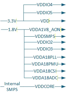
I am designing a custom board based on the STM32N657X0H3Q, using the STM32N6570-DK as a reference. The MCU is configured to use the internal SMPS for VCORE generation.
Unfortunately, my design does not fully comply with the recommended power sequencing described in the documentation:
- The various 1.8 V rails are generated from a single DC/DC converter.
- VDDA18USB, VDDA18CSI, and VDDA18ADC are powered directly from this 1.8 V rail.
- These rails are not gated by PWR_ON and therefore may become valid before or simultaneously with the PWR_ON assertion.
The MCU appears to boot and operate correctly during initial testing, but I would like to understand the implications of this deviation from the recommended power sequence.
My questions are:
- Does powering VDDA18USB, VDDA18CSI, and VDDA18ADC before (or independently of) PWR_ON create any risk of device damage or reduced reliability?
- Are there any known functional issues that could occur during startup, shutdown, or brownout conditions?
- Is this configuration considered acceptable when using the internal SMPS, provided all voltages remain within the specified limits?
- Has ST characterized or tested configurations where all 1.8 V domains are powered simultaneously from a common regulator?
Any guidance on the expected impact and long-term robustness of this power architecture would be greatly appreciated.
Thank you.