

Lin Zi
Associate II
May 30, 2018
Question

Monitoring the internal voltage reference

  • May 30, 2018
  • 8 replies
  • 3985 views
Posted on May 30, 2018 at 06:24

Hello ST engineers,

I have some questions about ADC of MCU STM32F302RC, please help to answer.

In our application, operating voltage of MCU is 3.3V (VDD=VDDA=3.3V). In firmware, we want to use VREFINT of ADC to calculate the VDDA to detect it.

According to the reference manual

http://www.st.com/content/ccc/resource/technical/document/reference_manual/16/bf/04/cd/f6/25/44/a7/DM00094349.pdf/files/DM00094349.pdf/jcr:content/translations/en.DM00094349.pdf

, section 15.3.32 (Monitoring the internal voltage reference) at page 353/1080 described how to calculate VDDA with VREFINT. Here is the formula,0690X0000060L0JQAU.png
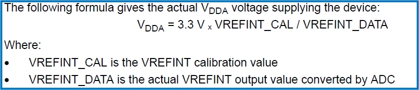
Under normal operation, there is no problem. The calculated value of VDDA is right, and the value is about 3.29V which is almost equal to the actual power supply voltage.

But as long as the input voltage of PA0 (TTa, this port is used as ADC function, channel is ADC1_IN1) is subjected to a voltage greater than 3.65V, such as 3.75V, the calculated value of VDDA will be abnormal and become to about 1.22V. My question are,

1), why this phenomena happen?

2), as long as any channel of ADC is subjected to a higher voltage (greater than 3.65V), the calculated value of VDDA based on this formula will be abnormal, such as become to 1.22V?

3), when a normal GPIO (no ADC function) of the MCU is input a voltage greater than 3.65V, will this phenomena happen?

Thank you in advance!

    This topic has been closed for replies.

    8 replies

    AvaTar
    Senior III
    May 30, 2018
    Posted on May 30, 2018 at 07:13

    Hello ST engineers,...

    Not sure how many ST engineer are present here.

    But as long as the input voltage of PA0 ... is subjected to a voltage greater than 3.65V, such as 3.75V, the calculated value of VDDA will be abnormal and become to about 1.22V.

    You are aware that you beyond specified limits, aren't you ? Proper functioning is not guaranteed.

    I think protective diodes at the input pins begin to open up.

    Lin Zi
    Lin ZiAuthor
    Associate II
    May 30, 2018
    Posted on May 30, 2018 at 07:55

    Hello Avatar,

    Thanks for reminding, this is a forum, any engineer can read this problem and can answer.

    Yes, because in the application, the condition of beyond specified limits can also happen, when the condition happened, the calculated value of VDDA become abnormal.

    you are right, under this condition, proper function is not guaranteed. And  what I want to know is that how the ADC will work when the input of ADC exceeds the upper limit? why it will affect the calculated value of VDDA? how does it affect the VDDA? etc.

    here is the internal block diagram of IO port when ADC function is used. I don't know if the 3.75V is enough to make the protection diode work. but it is not important, because from the test result, as long as the ADC port is input a voltage greater than 3.66V, the calculated value of VDDA will become abnormal, regardless of whether the clamp diode working.

    0690X0000060L1RQAU.png
    AvaTar
    Senior III
    May 30, 2018
    Posted on May 30, 2018 at 08:14

    ... any engineer can read this problem and can answer.

    My point is - only the ST engineers know the internal circuits and parameters.

    The others have to rely on official, published information, and guesses. Unfortunately, not many of  ST's engineering staff is present here.

    I used to protect my ADC inputs with a zener diode against excessive input voltages.

    And you could spare a second AIN, and apply a fraction of VDD (VDD/2 ... VDD/10), to see if VDD is within bounds.

    T J
    Senior III
    May 30, 2018
    Posted on May 30, 2018 at 08:03

    The protection diode is conducting and lifting your VDDA and so you will read a higher voltage,

    Don't exceed the VDD on any pin.  Otherwise your readings will be out.

    Its like a rule, you can break the rule, but you will suffer the issues.

    If you fix the problem, your issue will go away.

    You can use lower voltage protection diodes outside the chip and feed with a resistor.

    Lin Zi
    Lin ZiAuthor
    Associate II
    May 30, 2018
    Posted on May 30, 2018 at 08:33

    hello T J,

    Thank you for reply.

    1), first, I don't know if the diode can be conducted because of I don't know the Vf of the protection diode.

    2), second, even the diode is conducting, why the VDDA is lifted? from the test result, we found the actual VDDA (observed by an oscilloscope and a multi-meter) has not changed at all (always is 3.3V) when the calculated value of the VDDA is abnormal (only is 1.22V).

    3), use external diode with lower Vf (such as shottky diode), it is a good idea, but it is a protection method. in this topic, I still really want to know why this phenomena happened. in addition, for your suggestion of diode, we also tried before, and we found an interesting thing is that the lower Vf of diode you use, the higher leakage current of the diode. this also will cause some other issues, such as zero drift.

    thanks!

    T J
    Senior III
    May 30, 2018
    Posted on May 30, 2018 at 08:58

    the VDDA rail inside the processor must be affected, anyhow you can see the result.

    Stop the high voltage before it gets to the chip. <- this is your work, don't put water in the fuel tank, its a rule too.

    I use the ESD protection diodes, 2 diodes in one, and works for any pin. Something like this one.;

    https://www.digikey.com/product-detail/en/toshiba-semiconductor-and-storage/1SS295-TE85LF/1SS295-TE85LF-TR-ND/4304994


    normally you would use a resistor, maybe 100R before the diodes to protect the high current into the new diodes.