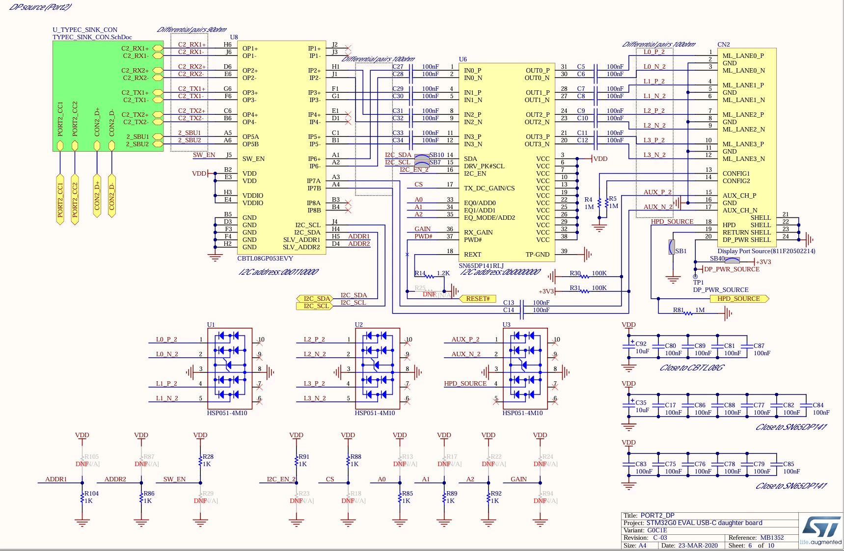
Mapping of four DP links and four sets of high-speed data lines between Type-C and DP
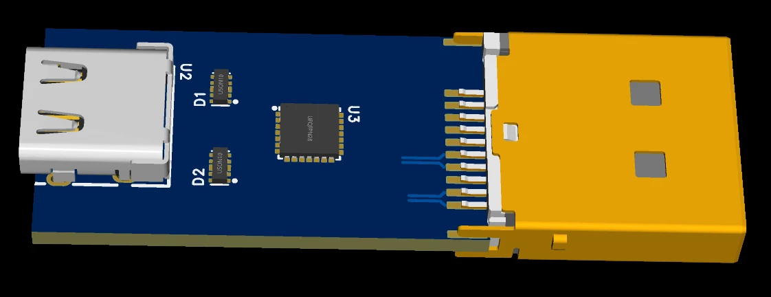
I'm planning to use an STM32G0 to make a Type-C to DP controller based on DP Alt Mode, and the high-speed data lines go straight to the DP links, but I'm not really sure how to connect them.Its shape would be something like this.
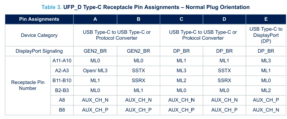
According to the pin assignment of TA0356, item E
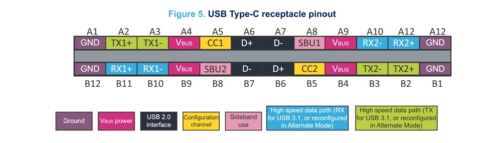
This is the Type-C socket definition I found from USB-IF
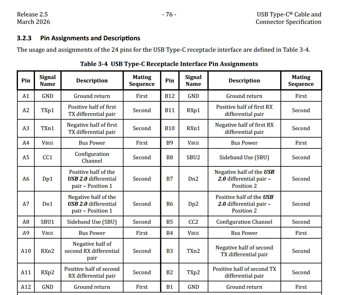
The mapping in TA0356 is shown in green font.
The DPLinks connections are
A2 - A3 = TX1 → ML1
B11-B10 = RX1 → ML0
B2 - B3 = TX2 → ML2
A11-A10 = RX2 → ML3
Third, this is VESA's PDF,
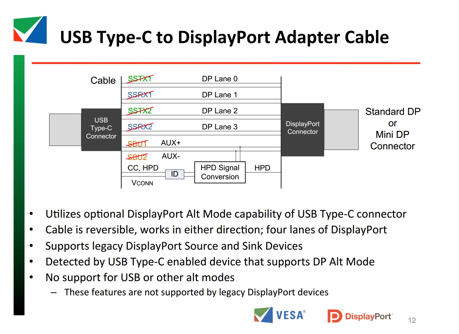
where PDPLinks correspond to shown in blue font.
TX1→ ML0
RX1→ ML1
TX2→ ML2
RX2→ ML3
Because in the VESA PDF it shows a Type-C cable adapter, we need to swap the TX and RX internally. This is mentioned in the USBIF PDF.
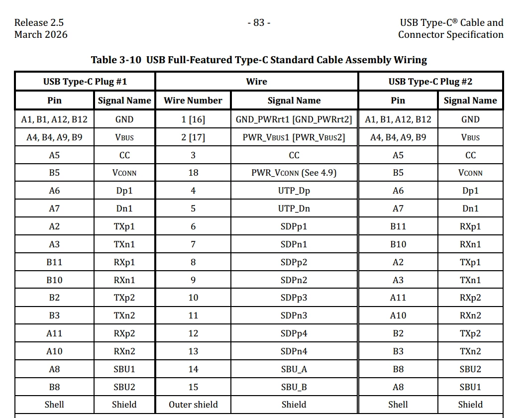
So, when the DPLinks in the VESA PDF switch to my design, the following changes will happen, shown in blue font.
TX1→ ML1
RX1→ ML0
TX2→ ML3
RX2→ ML2
After converting like this, I got a sequence of different DPLinks than in TA0356, where ML0 and ML1 are the same, and ML2 and ML3 are opposite.
TA0356 Ours
A2 - A3 = TX1 → ML1 TX1→ ML1
B11-B10 = RX1 → ML0 RX1→ ML0
B2 - B3 = TX2 → ML2 TX2→ ML3
A11-A10 = RX2 → ML3 RX2→ ML2
This might be related to the CtoC cable in the VESA PDF.Because the cables in here have the same sequence as the DPLinks on the TA0356.
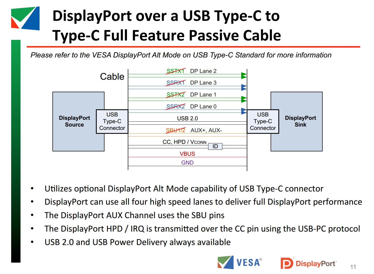
Finally, we also found an image error in TA0356. In Figure 5, there’s an extra A12 and a missing A11. Of course, it’s not a big deal.