

Associate II
August 3, 2026
Question

Is low impedance for the ADC input good or bad?

  • August 3, 2026
  • 3 replies
  • 20 views

I have noticed several recommendations on internet, that recommend providing a low high frequency impedance driving the ADC input for the MCU. For instance, you could add an RC-filter with the capacitance directly between the input pin and analog ground.


This is one of the recommendations:

https://community.st.com/stm32-mcus-products-25/many-people-have-complained-about-noise-on-adc-inputs-maybe-to-do-with-impedance-has-this-be-rectified-on-any-version-or-family-of-the-stm32-42573?tid=42573&fid=25


Well, I am not sure of such a recommendation anymore…


Perhaps I should just state that I am a novice regarding the use of STM32 processors, but I am old regarding general electronics design and electrical noise.


I have just tried this circuit with a Nucleo STM32G474RE board with 100 nF decoupling capacitor and a series resistor that I vary on the input pin:
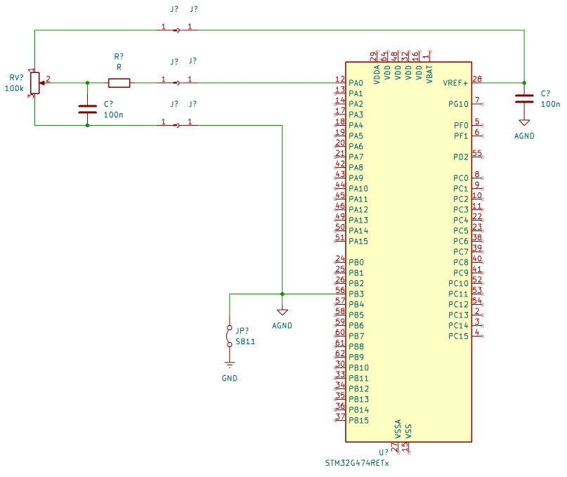


The preconditions are that I make an AD-conversion every second and with a 170 MHz sysclock and a 42.5 MHz ADC clock. The sample time is set to 12.5 clock cycles or 294 ns. No oversampling.


With the R-resistor set to 0 ohm, I get a peak-peak variation in the result value over one minute of about 33 LSB. When I change the resistor to 6.8 kOhm, the variation drops to about 12 LSB. It is about a 9 dB improvement.


I have also tried values of 3.3 kOhm and 12 kOhm, but then the noise tends to increase. So there seems to be a sweet spot here of this resistor value.


Some applications rightfully note that you should be aware of sufficient time for the internal SAR capacitors of the ADC to charge, and discharge from previous ADC conversion. I want to limit the previous charge to less than a ½ LSB of the 12 bits, and it is within 1/8192 in value, and you need 9 RC time constants for that. Therefore, you need a RC time constant below 294 ns/9 = 33 ns. According to datasheet the internal SAR capacitance is 5 pF. So, the calculated resistance becomes 6.5 kOhm – or close to the selected value of 6.8 kOhm.


I think that you can have some common GND wires inside the chip or some inductive coupling with high frequency spikes, that can change the charged value just before the sampling switches switches off. With a low driving impedance such a spike has larger influence on the remaining voltage on the SAR capacitance. The series resistor causes the SAR capacitance to act as a filter by itself and reduce this effect.


The test circuit I use is open with about 10 cm wires, so this is no proof. But if you are interested in lower noise at moderate conversion speeds, I think you should consider trying a series resistor there.
3 replies

AScha.3
Super User
August 3, 2026

Your wrong.

On these kind of ADC you always need low impedance at input, preferably a cer. cap with 10 or 100 nF direct to ground. 

If you want to know why, read about "charge redistribution ADC" , then you should understand.

The maximum impedance depends on sampling time and there is a table with values in the RM.

And have very short wire to the cap or impedance buffer amp, as on high resolution ADC you get many millivolts RF even on 50mm wire to ground.

"If you feel a post has answered your question, please click ""Accept as Solution""."
Visitor II
August 3, 2026

A low-impedance source is generally better for an ADC input because the ADC's internal sample-and-hold capacitor can charge more quickly and settle within the sampling time. The only trade-off is that an unnecessarily low impedance may increase power consumption in the driving circuit. If you're using a higher-impedance source, increasing the ADC sampling time or buffering the signal with an op-amp is often the recommended approach. It would also help to know whether you're measuring a slowly changing DC signal or a higher-speed analog signal.

waclawek.jan
Super User
August 3, 2026

The primary concern is that the measured value is not a true representation of input signal. Noise is somewhat secondary, and its reasons are more complex - IMO mostly crosstalk between the input signal and VREF+, possibly through ground impedance; but maybe other crostallks too. The ‘G4 ADC (or analog portion in general) in particular has its share of issues, as witnessed by ‘G4 ADC-related appnotes and the ‘G4-specific ADC appnote.

The concept of “let’s improve big output impedance of the signal source by using a huge capacitor” as a panacea is fundamentally flawed. Let’s assume you have the pot’s wiper at its middle, 50k, and the sampling capacitor is fully discharged at the beginning of sampling, which in practice is not, but we can’t be sure as there’s no guarantee for that and have to account for the worst case. That means that you are charging a 5pF capacitor to 1.5V each 294ns, that gives you an average current (smoothed out by the 100nF capacitor) of 5pF*1.5V/294ns = 25.5uA. That current is drawn through the 50kOhm portion of the pot, adding up to the “normal” divider current of 3V/100kOhm=30uA. Guess what’s the result.

For R>6.5kOhm this compounds with the fact that the sampling capacitor does not succeed to fully charge.

So, you either perform all these calculations for worst case, and change sampling rate accordingly; or spare yourself some disappointment and use an opamp-based buffer.

JW