Graham1904
Associate III
Mar 19, 2020 6:50 AM UTC
Solved

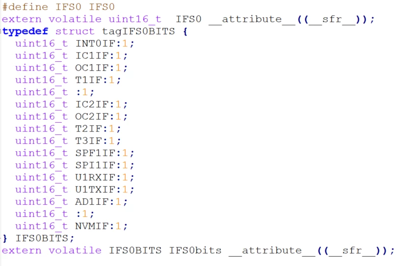
Having recently started with STM32 I am keen to get into programming in closer detail. Where can I find the "h" file defining the register list structure and the bit names as defined in the reference manual for the STM32F401RE ? see PIC24F32KA304 exa

0693W000000UHAXQA4.png

This topic has been closed for replies.
KnarfB
KnarfBBest answer
Super User
Mar 19, 2020 7:21 AM UTC

I'm using a different chip, but that doesn't matter much.

When creating a plain new Blinky project in STM32CubeIDE, the following folder structure is generated:

├───Core
│ ├───Inc
│ ├───Src
│ └───Startup
└───Drivers
 ├───CMSIS
 │ ├───Device
 │ │ └───ST
 │ │ └───STM32F0xx
 │ │ ├───Include
 │ │ └───Source
 │ │ └───Templates
 │ └───Include
 └───STM32F0xx_HAL_Driver
 ├───Inc
 │ └───Legacy
 └───Src

Register definitions belong to the vendor+MCU specific part of ARM CMSIS: Drivers\CMSIS\Device\ST\STM32F0xx\Include\stm32f042x6.h

The path may be slightly different when using other IDEs or command line build tools.

The definitions look a bit different, because no bit fields are used. Lets take a LED connected to GPIO Port B pin 3 for example. At first, port GPIOB must be switched on (which is typical for ARM devices):

RCC->AHBENR = RCC->AHBENR | RCC_AHBENR_GPIOBEN;

RCC (root clock complex) is an instance of type RCC_TypeDef at a fixed address RCC_BASE:

#define RCC ((RCC_TypeDef *) RCC_BASE)

Register AHBENR is defined as member of struct RCC_TypeDef in stm32f042x6.h:

typedef struct
{
 __IO uint32_t CR; /*!< RCC clock control register, Address offset: 0x00 */
 __IO uint32_t CFGR; /*!< RCC clock configuration register, Address offset: 0x04 */
 __IO uint32_t CIR; /*!< RCC clock interrupt register, Address offset: 0x08 */
 __IO uint32_t APB2RSTR; /*!< RCC APB2 peripheral reset register, Address offset: 0x0C */
 __IO uint32_t APB1RSTR; /*!< RCC APB1 peripheral reset register, Address offset: 0x10 */
 __IO uint32_t AHBENR; /*!< RCC AHB peripheral clock register, Address offset: 0x14 */
 __IO uint32_t APB2ENR; /*!< RCC APB2 peripheral clock enable register, Address offset: 0x18 */
 __IO uint32_t APB1ENR; /*!< RCC APB1 peripheral clock enable register, Address offset: 0x1C */
 __IO uint32_t BDCR; /*!< RCC Backup domain control register, Address offset: 0x20 */
 __IO uint32_t CSR; /*!< RCC clock control & status register, Address offset: 0x24 */
 __IO uint32_t AHBRSTR; /*!< RCC AHB peripheral reset register, Address offset: 0x28 */
 __IO uint32_t CFGR2; /*!< RCC clock configuration register 2, Address offset: 0x2C */
 __IO uint32_t CFGR3; /*!< RCC clock configuration register 3, Address offset: 0x30 */
 __IO uint32_t CR2; /*!< RCC clock control register 2, Address offset: 0x34 */
} RCC_TypeDef;

Further down you find definitions of the bit position

#define RCC_AHBENR_GPIOBEN RCC_AHBENR_GPIOBEN_Msk /*!< GPIOB clock enable */
#define RCC_AHBENR_GPIOCEN_Pos (19U) 
#define RCC_AHBENR_GPIOCEN_Msk (0x1UL << RCC_AHBENR_GPIOCEN_Pos) /*!< 0x00080000 */

Next, GPIOB pin 3 must be defined as push-pull output and finally the output must be set to high for switching the LED on. That part is left for you as an exercise 8).

A solution can be found here https://gitlab.com/stm32mcu/blinky_register-level

The STM32F0xx_HAL_Driver contains a higher level layer HAL (hardware abstrction layer). Its pros and cons are highly debated here.

hth

KnarfB

2 replies

KnarfB
KnarfBBest answer
Super User
Mar 19, 2020 7:21 AM UTC

I'm using a different chip, but that doesn't matter much.

When creating a plain new Blinky project in STM32CubeIDE, the following folder structure is generated:

├───Core
│ ├───Inc
│ ├───Src
│ └───Startup
└───Drivers
 ├───CMSIS
 │ ├───Device
 │ │ └───ST
 │ │ └───STM32F0xx
 │ │ ├───Include
 │ │ └───Source
 │ │ └───Templates
 │ └───Include
 └───STM32F0xx_HAL_Driver
 ├───Inc
 │ └───Legacy
 └───Src

Register definitions belong to the vendor+MCU specific part of ARM CMSIS: Drivers\CMSIS\Device\ST\STM32F0xx\Include\stm32f042x6.h

The path may be slightly different when using other IDEs or command line build tools.

The definitions look a bit different, because no bit fields are used. Lets take a LED connected to GPIO Port B pin 3 for example. At first, port GPIOB must be switched on (which is typical for ARM devices):

RCC->AHBENR = RCC->AHBENR | RCC_AHBENR_GPIOBEN;

RCC (root clock complex) is an instance of type RCC_TypeDef at a fixed address RCC_BASE:

#define RCC ((RCC_TypeDef *) RCC_BASE)

Register AHBENR is defined as member of struct RCC_TypeDef in stm32f042x6.h:

typedef struct
{
 __IO uint32_t CR; /*!< RCC clock control register, Address offset: 0x00 */
 __IO uint32_t CFGR; /*!< RCC clock configuration register, Address offset: 0x04 */
 __IO uint32_t CIR; /*!< RCC clock interrupt register, Address offset: 0x08 */
 __IO uint32_t APB2RSTR; /*!< RCC APB2 peripheral reset register, Address offset: 0x0C */
 __IO uint32_t APB1RSTR; /*!< RCC APB1 peripheral reset register, Address offset: 0x10 */
 __IO uint32_t AHBENR; /*!< RCC AHB peripheral clock register, Address offset: 0x14 */
 __IO uint32_t APB2ENR; /*!< RCC APB2 peripheral clock enable register, Address offset: 0x18 */
 __IO uint32_t APB1ENR; /*!< RCC APB1 peripheral clock enable register, Address offset: 0x1C */
 __IO uint32_t BDCR; /*!< RCC Backup domain control register, Address offset: 0x20 */
 __IO uint32_t CSR; /*!< RCC clock control & status register, Address offset: 0x24 */
 __IO uint32_t AHBRSTR; /*!< RCC AHB peripheral reset register, Address offset: 0x28 */
 __IO uint32_t CFGR2; /*!< RCC clock configuration register 2, Address offset: 0x2C */
 __IO uint32_t CFGR3; /*!< RCC clock configuration register 3, Address offset: 0x30 */
 __IO uint32_t CR2; /*!< RCC clock control register 2, Address offset: 0x34 */
} RCC_TypeDef;

Further down you find definitions of the bit position

#define RCC_AHBENR_GPIOBEN RCC_AHBENR_GPIOBEN_Msk /*!< GPIOB clock enable */
#define RCC_AHBENR_GPIOCEN_Pos (19U) 
#define RCC_AHBENR_GPIOCEN_Msk (0x1UL << RCC_AHBENR_GPIOCEN_Pos) /*!< 0x00080000 */

Next, GPIOB pin 3 must be defined as push-pull output and finally the output must be set to high for switching the LED on. That part is left for you as an exercise 8).

A solution can be found here https://gitlab.com/stm32mcu/blinky_register-level

The STM32F0xx_HAL_Driver contains a higher level layer HAL (hardware abstrction layer). Its pros and cons are highly debated here.

hth

KnarfB

Graham1904
Associate III
Mar 19, 2020 7:40 AM UTC

Absolutely fantastic. Thank you so much for your answer and the detail you have gone to the explain the solution. I found my file as being STM32F401xE.h :)

Using the on-chip temperature sensor I couldn't understand why the compiler kept complaining about TSVREFE not being previously defined, now i know why as it is ADC_CCR_TSVREFE :)

I have learnt so much from your answer. Thanks again.