Associate II
October 14, 2024
Solved

GPIO Trouble on STM32 F767ZI

I used a Nucleo F767ZI dev board to check and write firmware
(The IC on the board is STM32F767ZIT6U with the other characters being AA 254 VQ Z on first line and TWN AA 341 on line 2),
when I use HSI clock I am able to operate PD7, PG9, PG10, PG11, PG12 as an input or output GPIO
But on the custom developed board (the IC on the board is STM32F767ZIT6 with the other characters being AA108 VQ on the first line and TWN AA 334 on line two)

In this custom developed board while I am able to Program and debug the board and I am able to use all other pins except PD7, PG9, PG10, PG11, PG121)

1)The DC resistance of each of the above mentioned Pin and VCC(3V3) is infinite and same is with GND is also infinite

2) When I configure any of these Pins as GPIO Output as PUSH PULL and low speed mode then I see when I set the GPIO I see as the ODR setting but when I measure the voltage on the connecter(nothing between the connecter and the MCU Pin and tack length is less than 5 cms) i see 0.5 to 0.6V
3) When I configure any of these pins as Input with no Internal Pull or Pull Down, I see that these pins are not affected by noise where as other working pins are and if I connected 3V3 from a jumper cable to read input as logic High even that fails other than these 5 pins all other pins are working as expected.

Please help to debug the issue.

This topic has been closed for replies.
Chris21
Chris21Best answer
Associate II
October 15, 2024

This seems very likely to be involved:

"The VDDSDMMC is an independent power supply for SDMMC2 peripheral IOs (PD6, PD7,
PG9..12). It can be connected either to V DD or an external independent power supply."

Chris21_0-1729018282476.png


.

23 replies

Andrew Neil
Super User
October 14, 2024

@akash_praan wrote:

In this custom developed board


Please provide the schematics for this board.


A complex system that works is invariably found to have evolved from a simple system that worked.A complex system designed from scratch never works and cannot be patched up to make it work.
Associate II
October 15, 2024

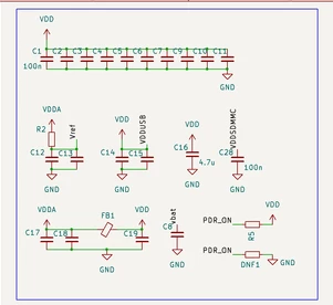
Hi @Andrew Neil , please find the schematic 

akash_praan_1-1728970300622.png

akash_praan_2-1728970347530.png


I am able to Program the board, 

GPIO Clock are defined (generated by Cube MX) properly, I am able to use all pins other than the 5 mentioned above. 
There is no extra component between the Pins and the connector and the length of each trace is also less than 6 to 7 cms. There is proper connectivity between the MCU pins and the connector Pads and Infinite DC Resistance between the MCU Pins and VCC, also between MCU Pins and GND

Surprisingly all 5 pins that don't work are connected between C28 and C6

akash_praan_0-1728970928764.png


Associate II
October 15, 2024

@Andrew Neil  Thank you for your time on this problem, if you need anything else to have a better understanding, please let me know. 

Andrew Neil
Super User
October 15, 2024

That's not a schematic - it doesn't show what is actually connected to the processor pins

A complex system that works is invariably found to have evolved from a simple system that worked.A complex system designed from scratch never works and cannot be patched up to make it work.
Associate II
October 15, 2024

@Andrew Neil Please find the required schematic parts for complete reference

. There is nothing between the MCU pin and the connector 

akash_praan_0-1729064259689.png


akash_praan_3-1729064316782.png


akash_praan_5-1729064364983.png


LCE
Principal III
October 15, 2024

So all these 5 pins are connected directly to the connector.

1) Have you removed the connector and then tested the GPIOs ?

2) Maybe the board / connector had some ESD stress? Was it assembled / used in an ESD-safe environment?

3) Do you have another board to check?

Richard Li
Senior
October 15, 2024

You need provide 1.8 v or 3.3v to vddsdmmc pin 132?

Richard Li
Senior
October 15, 2024

Pin 121

Associate II
October 15, 2024

https://www.st.com/en/microcontrollers-microprocessors/stm32f767zi.html
@Richard Li 
According to datasheet section 3.17, as per my understanding that needs to be done only when SDMMC i being used, but I will try connecting to 3.3V and then try it as all the mentioned pins which are not working have SDMMC as Alternate functions available. 

Thank you for you suggestion. 

@all please help me if my understanding is incorrect.

Associate II
October 15, 2024

Sure, I will try this out in the office in another 10 hours and see what the result. Most likely this should be it. 

Thank you for pointing this out. 

Regards,
Akash Rao

Richard Li
Senior
October 15, 2024

Beside the VDDSDMMC float, I don't understand why measure resistance for GND is like floating, You may need check pin 130 GND.

Chris21
Associate II
October 15, 2024

Another interesting observation.  Schematic only shows one VSS pin connected, ther should be 10.

.
Associate II
October 16, 2024

After the VDDSDMMC being connected, all pins work as intended. This was the error

VSS is internally connected as I verified in the Layout as well as the Hardware. 

Thank you for your help @Chris21 @Andrew Neil @LCE @Richard Li 

Chris21
Associate II
October 16, 2024

Not sure what you mean by: "VSS is internally connected".

ST's guidance:

All the power supply and ground pins must be properly connected to the power supplies.
These connections, including pads, tracks and vias should have as low impedance as
possible. This is typically achieved with thick track widths and, preferably, the use of
dedicated power supply planes in multilayer PCBs.


In addition, each power supply pair should be decoupled with filtering ceramic capacitors
(100 nF) and one single tantalum or ceramic capacitor (min. 4.7 μF) connected in parallel.
These capacitors need to be placed as close as possible to, or below, the appropriate pins
on the underside of the PCB. Typical values are 10 nF to 100 nF, but the exact values
depend on the application needs. Figure 23 shows the typical layout of such a VDD/VSS pair.

.
LCE
Principal III
October 16, 2024

> Not sure what you mean by: "VSS is internally connected".

The PCB layout screenshot shows that the GND pins are connected to GND underneath the package.

And some CAD apps' schematic symbols do not show all VCC or GND pins. I hate that, and rather draw my own...