

Lyu.1
Senior
August 19, 2024
Solved

CMOS- and TTL-compliant

Hi,Master:

platform: STM32G070CB

Quesion:
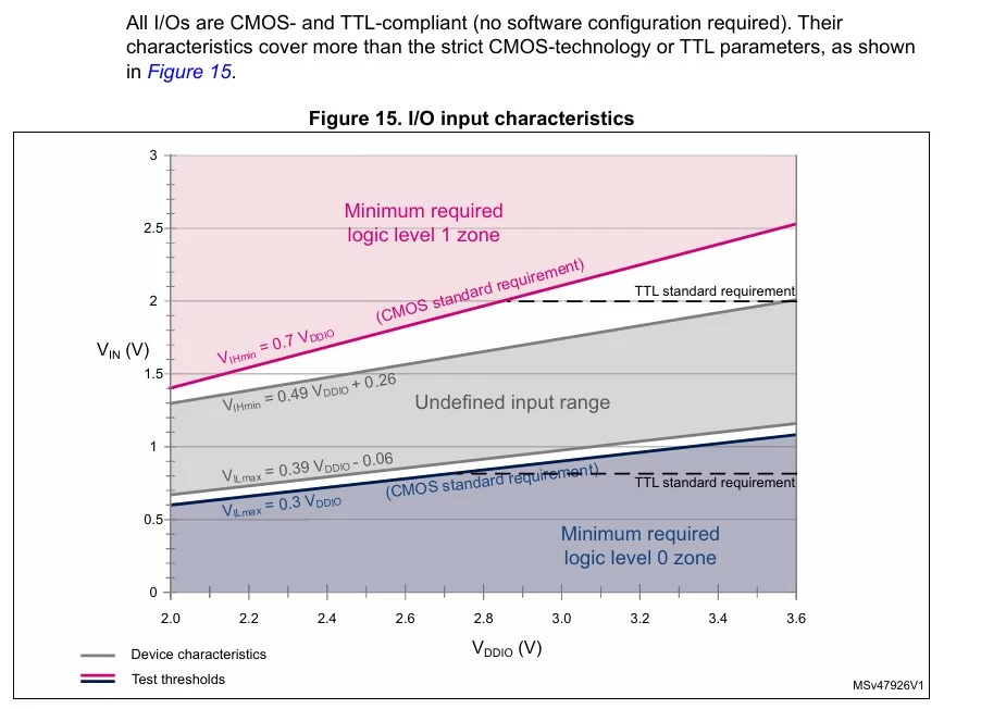
q.jpg


Regarding CMOS - and TTL compliant, the manual provides the above diagram. How does it achieve compatibility? When Vin>min (07 x VDDIO, 2), is it considered that the input is at a high level? When Vin<min (0.3 x VDDIO, 0.8), is the input considered low?

Thank you very much!

This topic has been closed for replies.
TDK
TDKBest answer
August 20, 2024

Refer to the "guaranteed by design" values in the datasheet, which correspond to regions outside of the gray zone in the picture. The G region is guaranteed by design to be logic high per this value in the datasheet.

TDK_0-1724121405518.png


"If you feel a post has answered your question, please click ""Accept as Solution""."

5 replies

TDK
August 19, 2024

> How does it achieve compatibility?

Above the gray region, the inputs are guaranteed to be read as high.

Below the gray region, the inputs are guaranteed to be read as low.

Because the requirements on CMOS/TTL (red and blue regions, plus/minus the region cut or added by the dashed line) have no overlap with the gray region, this chip satisfies CMOS/TTL requirements.

> When Vin>min (07 x VDDIO, 2), is it considered that the input is at a high level? When Vin<min (0.3 x VDDIO, 0.8), is the input considered low?

Yes

"If you feel a post has answered your question, please click ""Accept as Solution""."
Lyu.1
Lyu.1Author
Senior
August 20, 2024

Thanks. 

Is it also applicable for TT type pins (non-FT type)? For example, Vin > 0.8 but Vin < 0.3 x VDDIO are also considered low?

