Associate
Jan 16, 2026 12:12 AM UTC
Solved

About the pins and pin descriptions of the STM32H7S3A8I6

 Hello, I have a question about STM32H7S3A8I6 MCU.

https://www.st.com/resource/en/application_note/an5935-getting-started-with-stm32h7rx7sx-mcus-hardware-development-stmicroelectronics.pdf

Looking at Table 2 of the description in the PDF above, for graphics, STM32H7S3xx specifies GPU2D as N and GFXMMU as Y.

https://www.st.com/resource/en/datasheet/stm32h7s3a8.pdf

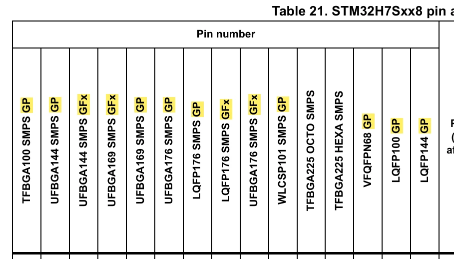
Looking at Table 21 in the following PDF, there are UFBGA 169 SMPS GFx and UFBGA 169SMPS GP. Can I look at the pin number with GFx?
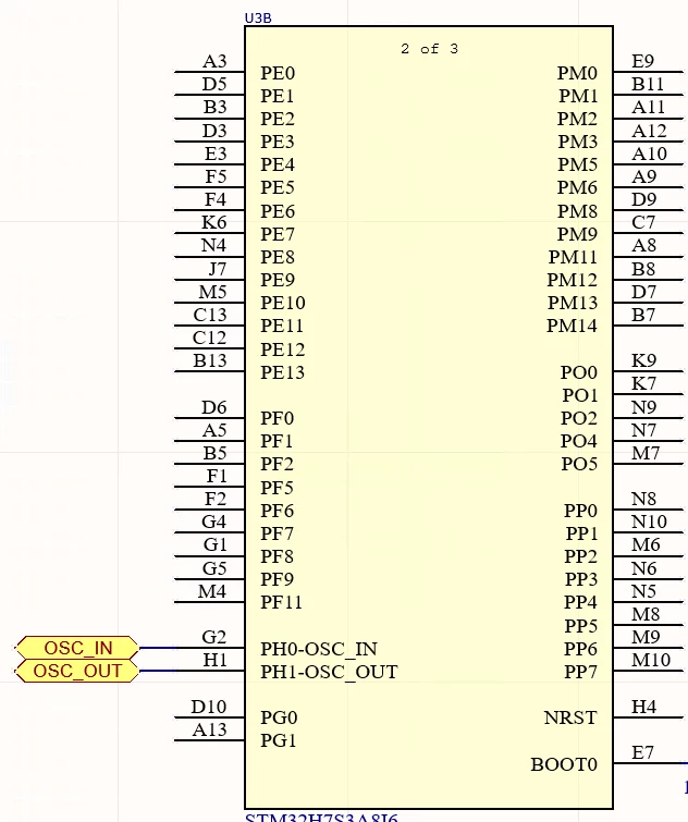
Woongi_0-1768522242502.png


and Is the library in the photo for the STM32H7S3A8I6 MCU?

TDK
TDKBest answer
Jan 16, 2026 2:47 AM UTC

The package has two dies, "GP" and "GFx", as do several other packages for that family. These have nothing to do directly with GPU2D or GFXMMU.

From the picture I showed in my previous reply, one can see that STM32H73S is a GP die, so that's what it lines up with.

TDK_0-1768531620384.png


"If you feel a post has answered your question, please click ""Accept as Solution""."

3 replies

TDK
Jan 16, 2026 12:26 AM UTC

The correct pinout for STM32H7S3A8I6 is Figure 8. UFBGA169 SMPS which lines up with UFBGA169 SMPS GP in Table 21.

TDK_0-1768523165012.png


"If you feel a post has answered your question, please click ""Accept as Solution""."
WoongiAuthor
Associate
Jan 16, 2026 12:53 AM UTC

@TDK  Thank you. Could you explain why? Or share some detailed documentation.

TDK
TDKBest answer
Jan 16, 2026 2:47 AM UTC

The package has two dies, "GP" and "GFx", as do several other packages for that family. These have nothing to do directly with GPU2D or GFXMMU.

From the picture I showed in my previous reply, one can see that STM32H73S is a GP die, so that's what it lines up with.

TDK_0-1768531620384.png


"If you feel a post has answered your question, please click ""Accept as Solution""."