Associate II
August 7, 2026
Question

STM32G431KB TIMER XOR ON/Hall Sensor Mode Not Triggering the PWM Timer

  • August 7, 2026
  • 26 replies
  • 137 views

Hello everyone,

I am working on a project where I need to control a BLDC motor with integrated hall sensors.

I saw this feature on RM0440 Document ‘29.3.28 Timer input XOR function’

I decided to use the TIM2 as the ‘Interfacing Timer’ and TIM1 as the PWM generating/motor driving timer.

I can read the time period between the hall sensor changes via TIM2->CCR1 register but I can not get the COM event with TIM1. Can anyone help?

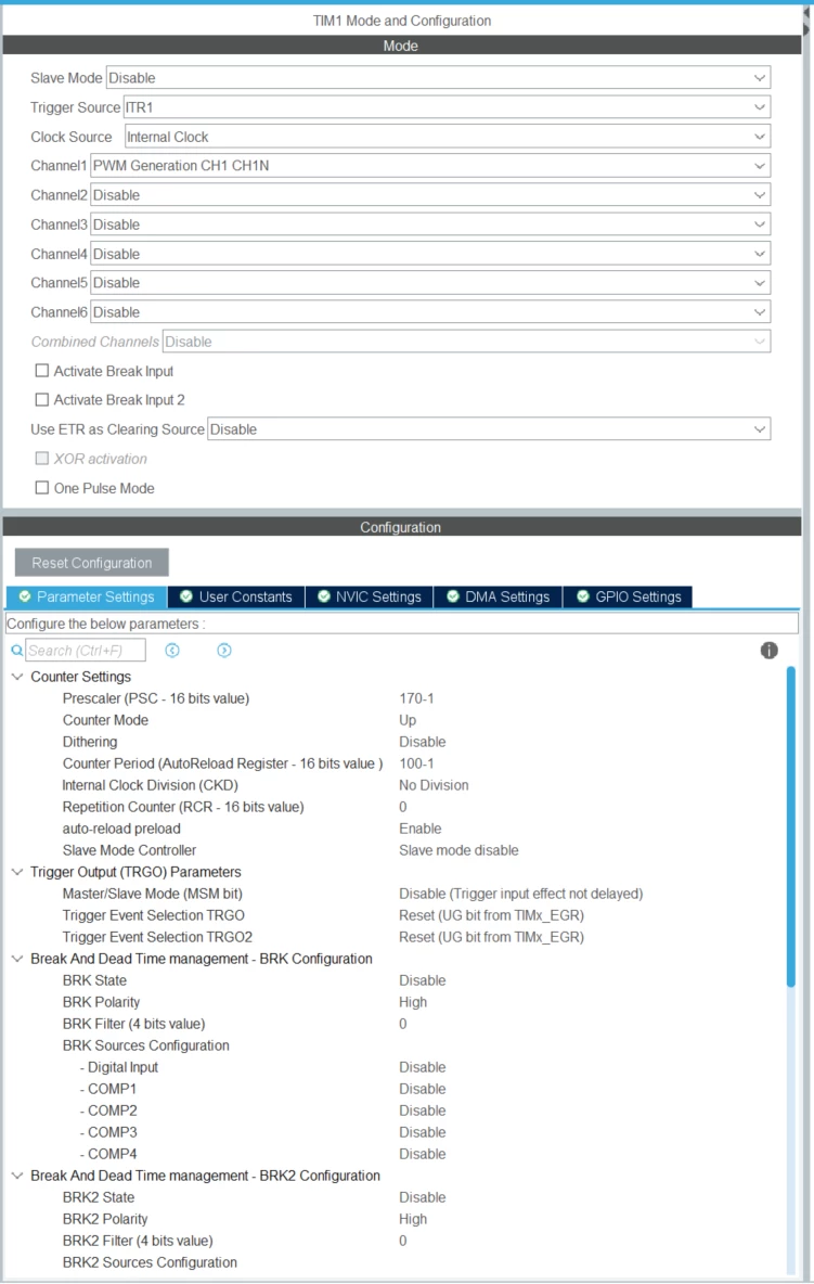
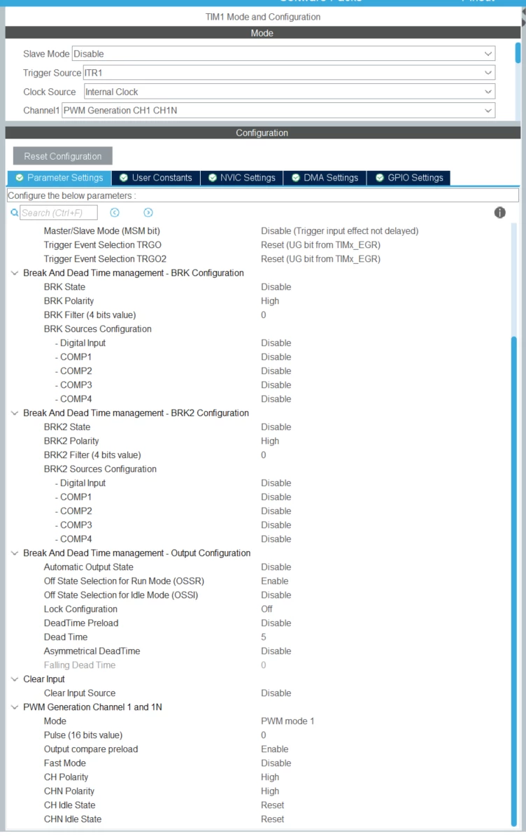
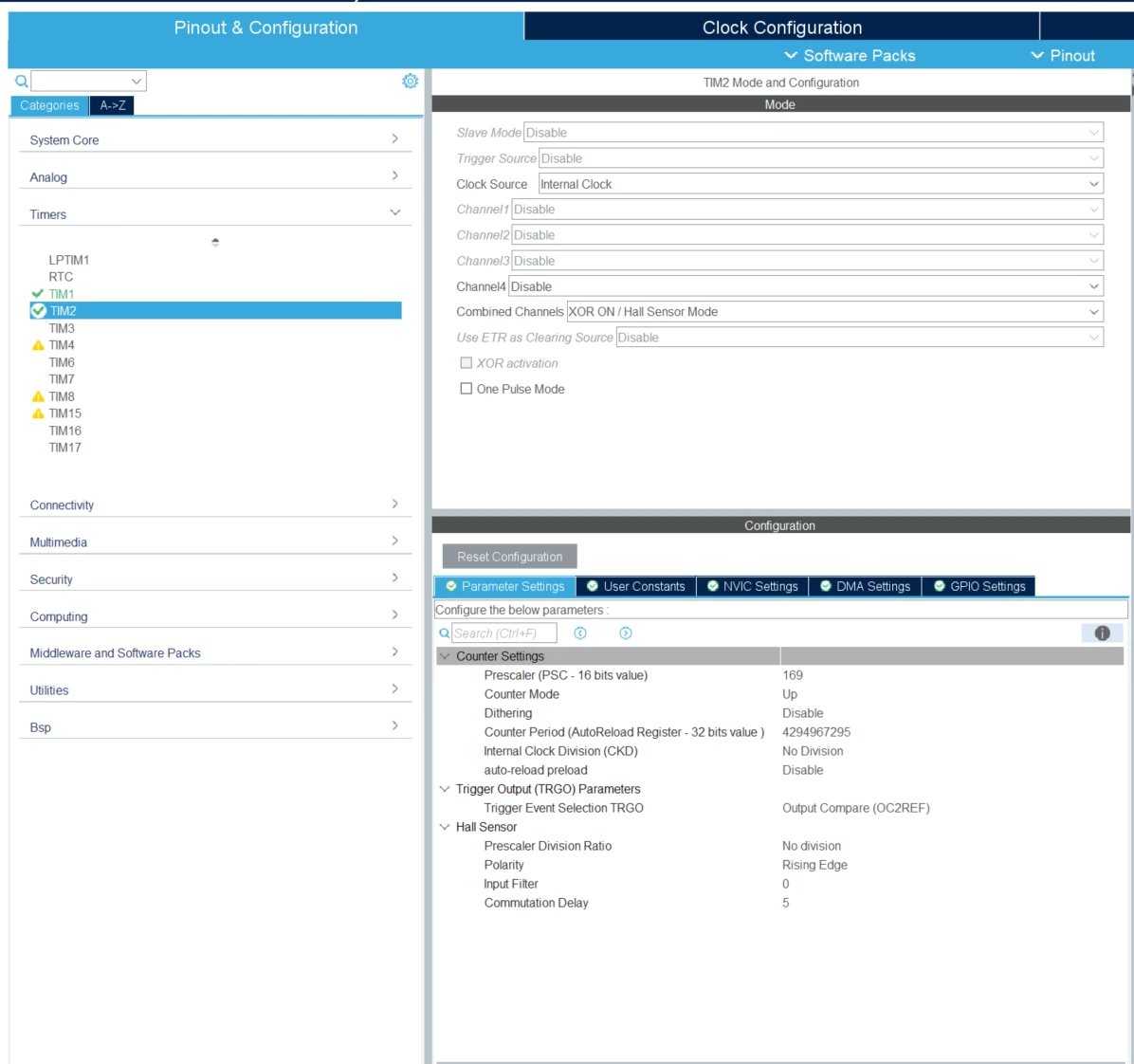
The following is my CUBEMX setup:


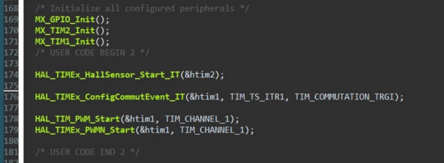
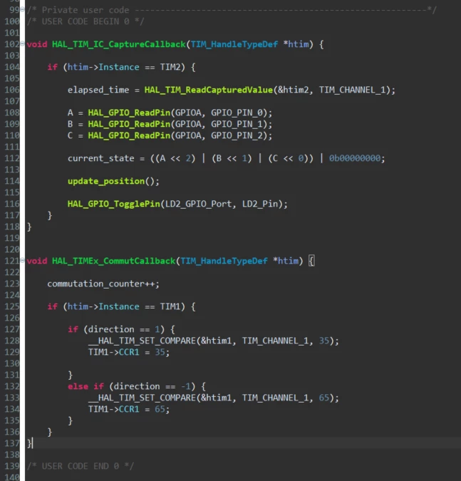
Here are the snippets of my code which I think are the most related. If you need other parts of my code I can provide it.


26 replies

waclawek.jan
Super User
August 7, 2026

> I can read the time period between the hall sensor changes via TIM2->CCR1 register 

So, why don’t you use CC1IF as TRGO source in TIM2 (TIM2->CR2.MMS = 0b011)?

JW

mdmrl00Author
Associate II
August 7, 2026

Hi, thanks for the answer.

But in the reference manual it says I should choose tim_oc2ref as the trigger source. And it’s the only one available to choose in the CUBEMX when I choose the XOR ON/Hall Sensor Mode for TIM2. Yes I can do it manually by registers but I am just trying to stay loyal to the reference manual.


waclawek.jan
Super User
August 7, 2026

OK so do you have this setup done? I.e. is TIM2’s slave-mode controller set to Reset, triggered by TI1F_ED, ARR to max, running freely? If you output TIM2_CH2 to a pin, do you see the waveform as per Fig.380?

Read out and check/post content of TIM2/TIM1 registers.

JW

mdmrl00Author
Associate II
August 7, 2026

I used CUBEMX to do the setup, when I select XOR ON/Hall Sensor Mode for TIM2, the option to select a different function for TIM2_CH2 is not possible on CUBE MX.

You can see it on the first image I posted. I can try setting up the process via registers. Is that what I need to do? Also I realized that in the reference manual 


In the instructions it says TIMx_CCMR1 register’s CC1S bits should be written to 01 thus tim_trc from the slave controller is selected as input capture signal. But in the TIMx_CCMR1 register description it says if we write 01 tim_ic1 gets connected to the tim_ti1.

Which one is correct here? Our trigger source comes from the slave mode controller or the tim_ti1 input?

waclawek.jan
Super User
August 7, 2026

In the instructions it says TIMx_CCMR1 register’s CC1S bits should be written to 01 thus tim_trc from the slave controller is selected as input capture signal. But in the TIMx_CCMR1 register description it says if we write 01 tim_ic1 gets connected to the tim_ti1.


Nice catch. It shows the quality of the documentation.

Both will work in some way - tim_ic1 is here output of the XOR (after filtering), tim_trc, given slave-mode controller is set to tim_ti1f_ed is output of edge detector of CH1. The behaviour then depends also on TIM2_CCER.CC1P/CC1NP settings.


I can try setting up the process via registers. Is that what I need to do?


I don’t use Cube/CubeMX, but I don’t want to force this to those who do. IMO the sensible thing here is to have a look at the timers’ registers (mostly TIM2), try to output TIM2_CH2 as I wrote above, and proceed from there. Post the registers here if you are unsure.

JW

mdmrl00Author
Associate II
August 8, 2026

First of all thank you for your interest and help. I really appreciate it.

Here is me following the reference manual steps and also decoding what I see from the SFR tab after ‘MX_TIM2_Init();’ function has ran.

Step 1: Configure three timer inputs ORed to the tim_ti1 input channel by writing the TI1S bit in the TIMx_CR2 register to 1.

Let’s check:

Here you can see the TI1S bit is set. This enables XOR gate which is outputted on the tim_ti1 signal line. Also MMS and MMS_1 bits total value comes as 0x5 = 0101 this means ‘tim_oc2ref signal is used as trigger output’ this is the last step in reference manual but I didn’t wanted to post the same picture twice. So just decoding it here.

Step 2: Program the time base: write the TIMx_ARR to the max value (the counter must be cleared by the tim_ti1 change. Set the prescaler to get a maximum counter period longer than the time between two changes on the sensors.

I set the PSC as 169 as the TIM2 runs at 170MHz to get a time-base of 1µs. I left the ARR register to it’s maximum value as recommended. Here is the picture:
 

Step 3: Program the channel 1 in capture mode (tim_trc selected): write the CC1S bits in the TIMx_CCMR1 register to 01. The digital filter can also be programmed if needed.

As you might remember this step was a bit suspicious. Because the reference manual says ‘tim_trc’ should be selected as input capture channel trigger by writing ‘01’ to the CC1S bits in the TIM2_CCMR1 register but in register description of CC1S bits in TIM2_CCMR1 register it says ‘tim_trc’ is selected as trigger source if only I write ‘11’ to CC1S bits.
While looking at the SFR tab I realized this step is written wrong in refence manual and yes the correct value to be written into CC1S bits is ‘11’ as it is what it can be seen from the SFR tab. Here it is:
 

CC1S is 0x3 = 11

The description is as following: CC1 channel is configured as input, tim_ic1 is mapped on tim_trc. This mode is working only if an internal trigger is selected through TS bit (TIMx_SMCR register). Note: CC1S bits are writable only when the channel is OFF (CC1E = 0 in TIMx_CCER).

So after all the init function does write ‘11’ to CC1S bits in TIM2_CCMR1 register. I also noticed the ‘IC2F’ bits set as 0x7, I checked this out and for some reason the digital filters gets set on their own. 0x7 = 0111 so this means:
 

 Also I thought I should also check out the TS bit in TIM2_SMCR register. Here is what I saw:
 

From here: TS = 0x4 and TS_1 = 0x0 combine them and I get 00100. This means, tim_ti1_ed is selected as the trigger input to the slave mode controller, right? Here are the bit field and 00100 value descriptions.

‘This bitfield selects the trigger input to be used to synchronize the counter.’
‘tim_ti1 edge detector (tim_ti1f_ed)’

Also the SMS = 0x4 and SMS_1 = 0x0 if we combine them: 0100. This stands for:

Reset mode- Rising edge of the selected trigger input (tim_trgi) reinitiazes the counter and generates an update of registers.’

So, as far as I know tim_ti1f_ed signal generates a rising edge signal everytime the XOR gate output toggles, am I right? Each time the XOR output toggles there is going to be a rising edge that’s going to fed into the slave mode controller.

Step 4: Program the channel 2 in PWM 2 mode with the desired delay: write the OC2M bits to 111 and the CC2S bits to 00 in the TIMx_CCMR1 register.

SFR shows: 

OC2M bits are 00 this means Capture Compare Channel 2 is configured as output. OC2M[12:3] bits are 0x7 and OC2M[24:1] = 0x0, combine them 0111. This means:

PWM mode 2 - In up-counting, channel 1 is inactive as long as TIMx_CNT<TIMx_CCR1 else active. In down-counting, channel 1 is active as long as TIMx_CNT>TIMx_CCR1 else inactive.

Step 5: Select tim_oc2ref as trigger output on tim_trgo: write the MMS bits in the TIMx_CR2
register to 101.

This was already done as it can be seen in the first picture. 

So far it seems everything is okay with TIM2. Can you also verify?

Thank you

Richard Li
Senior
August 7, 2026

As ​@waclawek.jan noticed, read back registers value after TIM1_Init and before PWM start, use STM32IDE ->debug→ read SFRs as attached picture


Richard Li
Senior
August 7, 2026

I am very interesting your project, if you locate in silicon valley,  I can join your project.

mdmrl00Author
Associate II
August 8, 2026

Thank you sir this means a lot. I will check what I see on the SFR tab and get back

Richard Li
Senior
August 8, 2026

In RM0440 Rev 9, page 32, as I attached, the XOR function only support TIM15.

This why CUBEMX doesn’t support,  looks you need change to TIM15.

Your debug is very good, only problem is, don’t dig so deep before check RM carefully, otherwise waste your time.

If any more questions, I like help.

mdmrl00Author
Associate II
August 8, 2026

But sir, I got it running on the TIM2 already, the problem here is that I cannot trigger the COM event on TIM1. Also I think you misunderstood the reference manual. In the section ‘30.4 TIM2/TIM3/TIM4/TIM5 functional description’ there is no warning as per the ‘30.4.21 Timer input XOR function’ so all the TIMERs specified here can be used for that mode. I also did this on TIM3 as well.


Richard Li
Senior
August 8, 2026

My bad, happy you passed TIM, your debug skill is very good, could you set break in callback, then looking for NVIC detail?

mdmrl00Author
Associate II
August 8, 2026

Let me see if I understand you clearly sir. I must put a breakpoint in the input capture callback for the TIMER2, correct?


Here is my callback

This function gets triggered when I spin the hall sensored motor with an external controller. I extended another cable from the sensor outputs of the motor to my STM32G431KB-Nucleo to read them.

Richard Li
Senior
August 8, 2026

You can try, but I think should add in HAL_TIMx_Commut_Callback, your event didn’t come out, so I guess interrupt didn’t go though. 

Richard Li
Senior
August 8, 2026

For my debug, need try every possibility if not damage something.

Other people suggestion only try help you, and they don’t like you got more real information. 

So may misguide you, give you wrong instruction. 

Richard Li
Senior
August 8, 2026

Most important is NVIC, for my understanding, callback use NVIC. Beside RM0440 , you need read PM0214.

mdmrl00Author
Associate II
August 8, 2026

I am not really familiar with register based programming and NVIC architecture but I’ll try to decode what’s going on. Right now I don’t quite understand why I get 2 commutation events per hall sensor change.

Richard Li
Senior
August 8, 2026

My English no good, and some my answer may sounds rude, please ignore those, Do you know interrupt?

Richard Li
Senior
August 8, 2026

BYW, don’t need “sir”, engineer job is solve problem, don’t care other people like or not, it just like play one game, after finish, fell good by myself.

mdmrl00Author
Associate II
August 8, 2026

I understand. Thank you so much for helping this far