

Generating PWM signal and GPIO ON state from the same pin periodically.
Hello everyone,
I’m interested in electric motor drives and power electronics. I’m trying to create a C program for STM32F407 Discovery board that executes Hall sensored 6 step commutation with complementary PWM.
The program must apply a PWM signal to the high side mosfet, complement of this pwm signal to same leg low side mosfet with significant dead time and GPIO-ON State to corresponding low side mosfet according to Hall sensor state. You can see what I’m trying to do in the figure below.
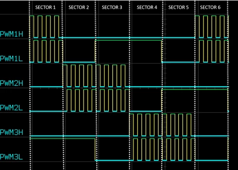
I set the GPIO pins to alternate function to generate PWM and did necessary configuration to generate complement of this PWM signal. But I’m confused. For instance at sector 1, I generated both PWM signals and control the PWM3L via GPIOx->ODR register. But at sector 4 I need to apply PWM signal for the same pin(PWM3L). Do I need to configure the pin as output or alternate function? How can I configure this? Do I need to use event or interrupt. Can anyone help me please? Thanks in advance. I leave the program that impelement complementary PWM signal with 8us dead time.
void GPIO_Init(void)
{
 RCC->AHB1ENR |= (1U<<0) | (1U<<2) ; /*GPIOA and GPIOC clock enable*/
 GPIOA ->MODER |= (1U<<11); /*PA5 set as alternate func*/
 GPIOA->MODER &=~ (1U<<10) ;
 GPIOC->MODER |= (1U<<13) ; /*PC6 set as alternate func*/
 GPIOC->MODER &=~ (1U<<12) ;
 GPIOA->AFR[0] |= (1U<<21) ;
 GPIOA->AFR[0] |= (1U<<20) ; /*PA5---->AF03----TIM8_CH1N*/
 GPIOA->AFR[0] &=~(1U<<19);
 GPIOA->AFR[0] &=~(1U<<18);
 GPIOC->AFR[0] |= (1U<<25);
 GPIOC->AFR[0] |= (1U<<24); /*PC6---->AF03----TIM8_CH1*/
 GPIOC->AFR[0] &=~ (1U<<26);
 GPIOC->AFR[0] &=~ (1U<<27);
}

void PWM_Init(void)
{
 RCC->APB2ENR |= (1U<<1); /*TIM8 clock enable*/
 TIM8->PSC = 16-1; /*16 000 000 / 16 = 1 000 000 Hz = 1us period*/
 TIM8->ARR =1000-1 ; /*1ms period*/
 TIM8->CCR1 = 250-1; /*%25 duty*/
 TIM8->CCER |= (1U<<0);
 TIM8->CCER |= (1U<<2);
 TIM8->CCER &=~ (1U<<1); /*OC1 and OC1N output polarity*/
 TIM8->CCER &=~ (1U<<3);
 TIM8->BDTR |= (0x887F) ; /*MOE , OSSR bits and dead time calculation*/
 TIM8->CCMR1 |= (1U<<6);
 TIM8->CCMR1 |= (1U<<5); /*PWM mode 1 */
 TIM8->CCMR1 &=~ (1U<<4);
 TIM8->CNT = 0; /*Initialize counter*/
 TIM8->CR2 |= (1U<<0); /*CCPC*/
 TIM8->CR2 &=~ (1U<<8); /*output Idle of OC1 state zero*/
 TIM8->CR2 |= (1U<<9) ; /*Output Idle state of OC1N*/
 TIM8->CR1 |= (1U<<0); /*counter enable*/
}