Solved
STM32L496ZGT6 internal regulator output voltage
Hi
I have a problem with my board with STM32L496ZGT6.
Some boards works fine (so.. i think there isn't a project problem) some boards are in loop during the power on.
I exaplin better:
Here a function in main.cpp:
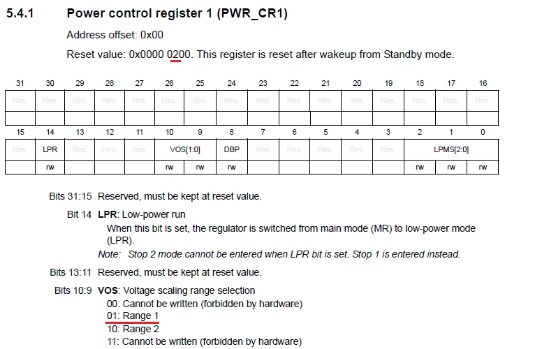
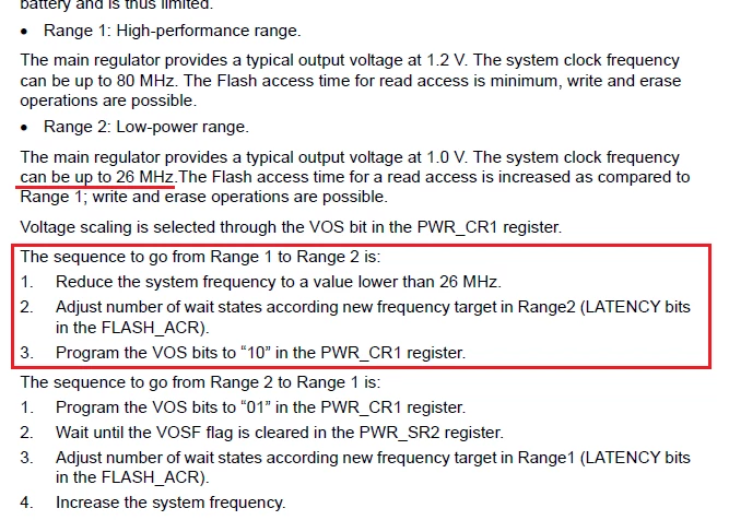
	/*Configure the main internal regulator output voltage...............................................*/
	if (HAL_PWREx_ControlVoltageScaling(PWR_REGULATOR_VOLTAGE_SCALE2) != HAL_OK)
	{
		_Error_Handler(__FILE__, __LINE__);
	}
void _Error_Handler(char *, int)
{
	while(1){}
}
If I comment:
	/*Configure the main internal regulator output voltage...............................................*/
	/*
	if (HAL_PWREx_ControlVoltageScaling(PWR_REGULATOR_VOLTAGE_SCALE2) != HAL_OK)
	{
		_Error_Handler(__FILE__, __LINE__);
	}
	/*.....
The board power on reguarly so it means:
HAL_PWREx_ControlVoltageScaling(PWR_REGULATOR_VOLTAGE_SCALE2) != 0
This is esay but why does this happen?
Hardware problem?
Here the function HAL_PWREx_ControlVoltageScaling:
HAL_StatusTypeDef HAL_PWREx_ControlVoltageScaling(uint32_t VoltageScaling)
{
 uint32_t wait_loop_index = 0;

 assert_param(IS_PWR_VOLTAGE_SCALING_RANGE(VoltageScaling));

#if defined(PWR_CR5_R1MODE)
 if (VoltageScaling == PWR_REGULATOR_VOLTAGE_SCALE1_BOOST)
 {
 /* If current range is range 2 */
 if (READ_BIT(PWR->CR1, PWR_CR1_VOS) == PWR_REGULATOR_VOLTAGE_SCALE2)
 {
 /* Make sure Range 1 Boost is enabled */
 CLEAR_BIT(PWR->CR5, PWR_CR5_R1MODE);

 /* Set Range 1 */
 MODIFY_REG(PWR->CR1, PWR_CR1_VOS, PWR_REGULATOR_VOLTAGE_SCALE1);

 /* Wait until VOSF is cleared */
 wait_loop_index = (PWR_FLAG_SETTING_DELAY_US * (SystemCoreClock / 1000000));
 while ((wait_loop_index != 0) && (HAL_IS_BIT_SET(PWR->SR2, PWR_SR2_VOSF)))
 {
 wait_loop_index--;
 }
 if (HAL_IS_BIT_SET(PWR->SR2, PWR_SR2_VOSF))
 {
 return HAL_TIMEOUT;
 }
 }
 /* If current range is range 1 normal or boost mode */
 else
 {
 /* Enable Range 1 Boost (no issue if bit already reset) */
 CLEAR_BIT(PWR->CR5, PWR_CR5_R1MODE);
 }
 }
 else if (VoltageScaling == PWR_REGULATOR_VOLTAGE_SCALE1)
 {
 /* If current range is range 2 */
 if (READ_BIT(PWR->CR1, PWR_CR1_VOS) == PWR_REGULATOR_VOLTAGE_SCALE2)
 {
 /* Make sure Range 1 Boost is disabled */
 SET_BIT(PWR->CR5, PWR_CR5_R1MODE);

 /* Set Range 1 */
 MODIFY_REG(PWR->CR1, PWR_CR1_VOS, PWR_REGULATOR_VOLTAGE_SCALE1);

 /* Wait until VOSF is cleared */
 wait_loop_index = (PWR_FLAG_SETTING_DELAY_US * (SystemCoreClock / 1000000));
 while ((wait_loop_index != 0) && (HAL_IS_BIT_SET(PWR->SR2, PWR_SR2_VOSF)))
 {
 wait_loop_index--;
 }
 if (HAL_IS_BIT_SET(PWR->SR2, PWR_SR2_VOSF))
 {
 return HAL_TIMEOUT;
 }
 }
 /* If current range is range 1 normal or boost mode */
 else
 {
 /* Disable Range 1 Boost (no issue if bit already set) */
 SET_BIT(PWR->CR5, PWR_CR5_R1MODE);
 }
 }
 else
 {
 /* Set Range 2 */
 MODIFY_REG(PWR->CR1, PWR_CR1_VOS, PWR_REGULATOR_VOLTAGE_SCALE2);
 /* No need to wait for VOSF to be cleared for this transition */
 /* PWR_CR5_R1MODE bit setting has no effect in Range 2 */
 }

#else

 /* If Set Range 1 */
 if (VoltageScaling == PWR_REGULATOR_VOLTAGE_SCALE1)
 {
 if (READ_BIT(PWR->CR1, PWR_CR1_VOS) != PWR_REGULATOR_VOLTAGE_SCALE1)
 {
 /* Set Range 1 */
 MODIFY_REG(PWR->CR1, PWR_CR1_VOS, PWR_REGULATOR_VOLTAGE_SCALE1);

 /* Wait until VOSF is cleared */
 wait_loop_index = (PWR_FLAG_SETTING_DELAY_US * (SystemCoreClock / 1000000));
 while ((wait_loop_index != 0) && (HAL_IS_BIT_SET(PWR->SR2, PWR_SR2_VOSF)))
 {
 wait_loop_index--;
 }
 if (HAL_IS_BIT_SET(PWR->SR2, PWR_SR2_VOSF))
 {
 return HAL_TIMEOUT;
 }
 }
 }
 else
 {
 if (READ_BIT(PWR->CR1, PWR_CR1_VOS) != PWR_REGULATOR_VOLTAGE_SCALE2)
 {
 /* Set Range 2 */
 MODIFY_REG(PWR->CR1, PWR_CR1_VOS, PWR_REGULATOR_VOLTAGE_SCALE2);
 /* No need to wait for VOSF to be cleared for this transition */
 }
 }
#endif

 return HAL_OK;
}
Any advice?